PEM · 2018-12-17 · VIGO SYSTEM S.A. 129/133 Poznańska St. 05-850 Ożarów Mazowiecki, Poland...
2
www.vigo.com.pl VIGO SYSTEM S.A. 129/133 Poznańska St. 05-850 Ożarów Mazowiecki, Poland phone: +48 22 733 54 10 fax: +48 22 733 54 26 [email protected] MCT Photoelectromagnetic detectors The PEM series detectors operate on the photoelectromagnetic effect in the semiconductors. The devices are typi- cally optimized for the best performance at 10.6 μm. Example of D* vs Wavelength λ for PC Series HgCdTe Detectors. Spectral Characteristics of individual detectors may vary from those shown on the chart. IR Detector Specification @20°C Detector type Cooling, operang temperature [ ] TK Opmal wavelengt h *) [ ] opt m λ µ Detecvity **) Current responsivity length product @λ opt Time constant Resistance [ ] R Ω Acceptance angle Opcal area ***) Package Window ****) @λ peak @λ opt PEM uncooled, ~ 300 10.6 ≥1.6×10 7 ≥1.0×10 7 ≥0.002 ≤1.2 40 to 100 ~ 48, 1.23 1×1 2×2 PEM-SMA, PEM-TO8 wedged ZnSe AR coated *) Other optimal wavelengths available upon request. **) Data sheet states minimum guaranteed D* values for each detector model. Higher performance detectors can be provided upon request. ***) Other optical areas available upon request. **** ) Other windows available upon request. 1 ) Optical area available only for uncooled detectors PEM Detector code description Features: › Ambient temperature operation › No bias required › 2 to 11 μm spectral range › Time constant of 1 ns or less › No flicker noise › Operation from DC to VHF › Lightweight, rugged and reliable › Convenient to use › Low cost › Custom design upon request Detector package Window (without window) FOV VIGO detector type Optimal wavelength Optical area PEM 10.6 1x1 BNC NoWindow 102 1E+06 1E+07 1E+08 2 3 4 5 6 7 8 9 10 11 D* [c 1/2 -1 m·Hz ·W ] λ [μm] 10.6μm
Transcript of PEM · 2018-12-17 · VIGO SYSTEM S.A. 129/133 Poznańska St. 05-850 Ożarów Mazowiecki, Poland...
www.vigo.com.pl VIGO SYSTEM S.A.129/133 Poznańska St.05-850 Ożarów Mazowiecki, Poland
phone: +48 22 733 54 10 fax: +48 22 733 54 26
MCT Photoelectromagnetic detectors
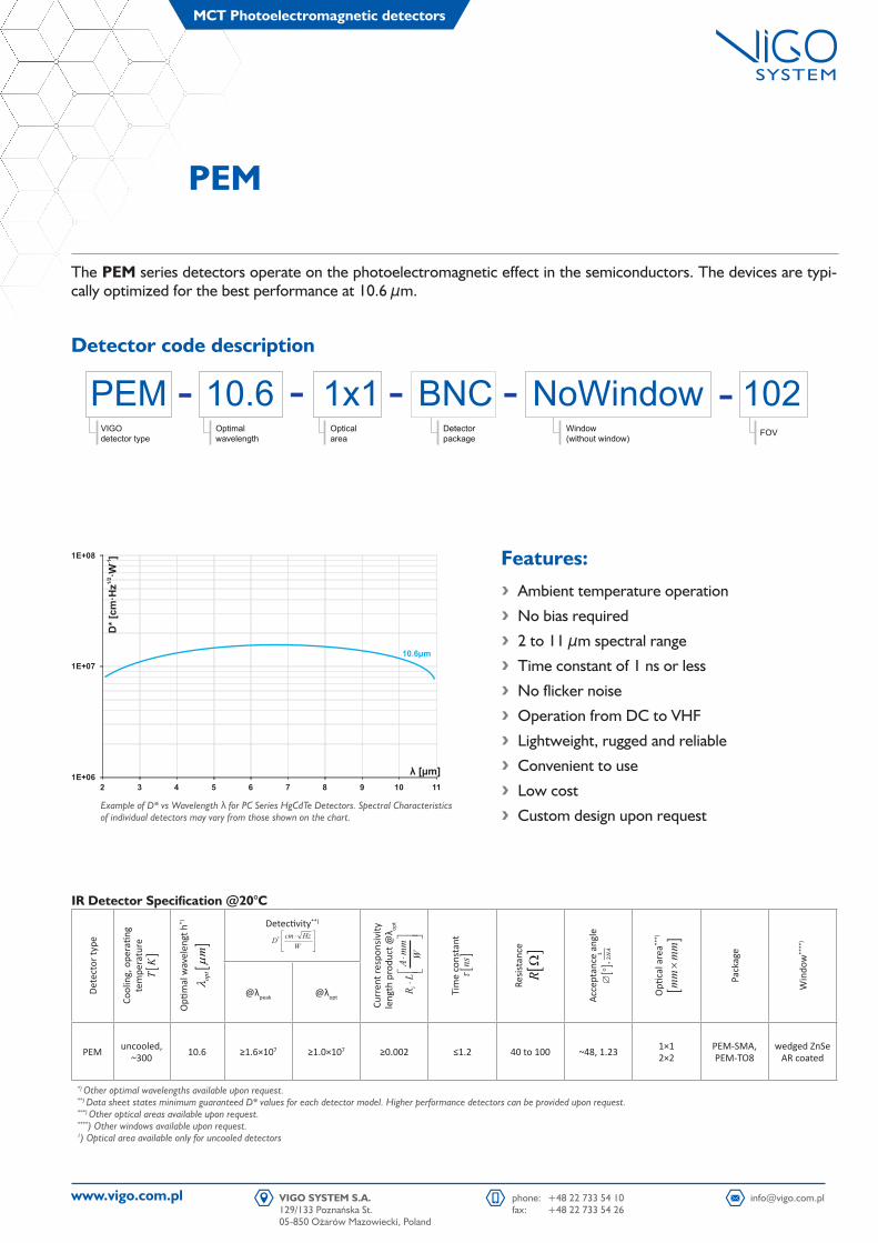
The PEM series detectors operate on the photoelectromagnetic effect in the semiconductors. The devices are typi-cally optimized for the best performance at 10.6 μm.
Example of D* vs Wavelength λ for PC Series HgCdTe Detectors. Spectral Characteristics of individual detectors may vary from those shown on the chart.
IR Detector Specification @20°C
Dete
ctor
type
Cool
ing,
ope
ratin
g te
mpe
ratu
re
[]
TK
Opti
mal
wav
elen
gt h
*)
[]
opt
mλ
µ
Detectivity**)
Curr
ent r
espo
nsiv
ity
leng
th p
rodu
ct @
λ opt
Tim
e co
nsta
nt
Resis
tanc
e
[]
RΩ
Acce
ptan
ce a
ngle
Opti
cal a
rea**
*)
Pack
age
Win
dow
****
)
@λpeak @λopt
PEM uncooled, ~300 10.6 ≥1.6×10⁷ ≥1.0×10⁷ ≥0.002 ≤1.2 40 to 100 ~48, 1.23 1×1
2×2PEM-SMA, PEM-TO8
wedged ZnSe AR coated
*) Other optimal wavelengths available upon request.**) Data sheet states minimum guaranteed D* values for each detector model. Higher performance detectors can be provided upon request.***) Other optical areas available upon request.****) Other windows available upon request.1) Optical area available only for uncooled detectors
PEM
Detector code description
Features: › Ambient temperature operation
› No bias required
› 2 to 11 μm spectral range
› Time constant of 1 ns or less
› No flicker noise
› Operation from DC to VHF
› Lightweight, rugged and reliable
› Convenient to use
› Low cost
› Custom design upon request
Detector package
Window(without window)
FOVVIGOdetector type
Optimal wavelength
Optical area
PEM 10.6 1x1 BNC NoWindow 102
1E+06
1E+07
1E+08
2 3 4 5 6 7 8 9 10 11
D*
[c1
/2-1
m·H
z·W
]
λ [µm]
10.6µm
www.vigo.com.pl VIGO SYSTEM S.A.129/133 Poznańska St.05-850 Ożarów Mazowiecki, Poland
phone: +48 22 733 54 10 fax: +48 22 733 54 26
MCT Photoelectromagnetic detectors
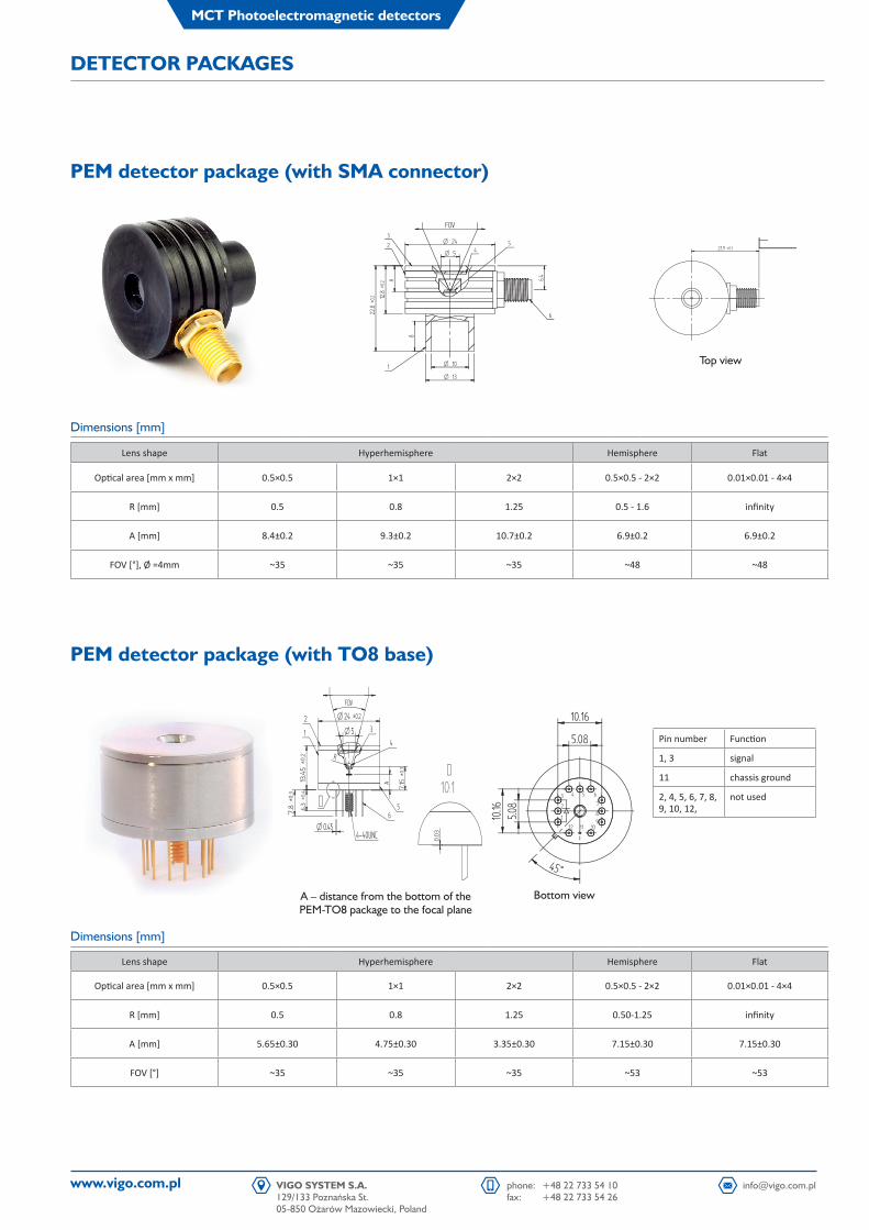
DETECTOR PACKAGES
PEM detector package (with SMA connector)
Top view
Dimensions [mm]
Lens shape Hyperhemisphere Hemisphere Flat
Optical area [mm x mm] 0.5×0.5 1×1 2×2 0.5×0.5 - 2×2 0.01×0.01 - 4×4
R [mm] 0.5 0.8 1.25 0.5 - 1.6 infinity
A [mm] 8.4±0.2 9.3±0.2 10.7±0.2 6.9±0.2 6.9±0.2
FOV [°], Ø =4mm ~35 ~35 ~35 ~48 ~48
PEM detector package (with TO8 base)
A – distance from the bottom of the PEM-TO8 package to the focal plane
Bottom view
Pin number Function
1, 3 signal
11 chassis ground
2, 4, 5, 6, 7, 8, 9, 10, 12,
not used
Dimensions [mm]
Lens shape Hyperhemisphere Hemisphere Flat
Optical area [mm x mm] 0.5×0.5 1×1 2×2 0.5×0.5 - 2×2 0.01×0.01 - 4×4
R [mm] 0.5 0.8 1.25 0.50-1.25 infinity
A [mm] 5.65±0.30 4.75±0.30 3.35±0.30 7.15±0.30 7.15±0.30
FOV [°] ~35 ~35 ~35 ~53 ~53