
Tesis Doctoral MODELADO DE FENOMENOS´ DE HISTERESIS Y ...hera.ugr.es/tesisugr/21947089.pdf · to...
161
Tesis Doctoral MODELADO DE FEN ´ OMENOS DE HIST ´ ERESIS Y CONTACTOS EN TRANSISTORES ORG ´ ANICOS/POLIM ´ ERICOS. Autor: KARAM MOHAMMAD AWAWDEH Director: Juan Antonio Jim ´ enez Tejada Programa Oficial de Posgrado en F´ ısica Dept. Electr´ onica y Tecnolog´ ıa de Computadores Universidad de Granada 2013
Transcript of Tesis Doctoral MODELADO DE FENOMENOS´ DE HISTERESIS Y ...hera.ugr.es/tesisugr/21947089.pdf · to...

Tesis Doctoral
MODELADO DE FENOMENOS
DE HISTERESIS Y
CONTACTOS EN
TRANSISTORES
ORGANICOS/POLIMERICOS.
Autor:
KARAM MOHAMMAD AWAWDEH
Director:
Juan Antonio Jimenez Tejada
Programa Oficial de Posgrado en Fısica
Dept. Electronica y Tecnologıa de
Computadores
Universidad de Granada
2013

Editor: Editorial de la Universidad de GranadaAutor: Karam Mohammad AwawdehD.L.: GR 2223-2013ISBN: 978-84-9028-653-1


El doctorando KARAM AWAWDEH y el director de la tesis JUAN ANTONIO
JIMENEZ TEJADA garantizamos, al firmar esta tesis doctoral, que el trabajo ha si-
do realizado por el doctorando bajo la direccion del director de la tesis, y hasta donde
nuestro conocimiento alcanza, en la realizacion del trabajo, se han respetado los derechos
de otros autores a ser citados, cuando se han utilizado sus resultados o publicaciones.
Granada, 25 de febrero de 2013
Director/es de la Tesis Doctorando
Fdo.: Juan Antonio Jimenez Tejada Fdo.: Karam Awawdeh


Dr. Juan A. Jiménez Tejada, Catedrático de Universidad del Departamento de Electrónica y Tecnología de Computadores de la Universidad de Granada. CERTIFICA Que el trabajo de investigación que se recoge en la presente Memoria, titulada " MODELADO DE FENÓMENOS DE HISTÉRESIS Y CONTACTOS EN TRANSISTORES ORGÁNICOS/ POLIMÉRICOS." presentada por D. Karam Awawdeh para optar al grado de Doctor, ha sido realizado en su totalidad bajo su dirección en el Departamento de Electrónica y Tecnología de Computadores de la Universidad de Granada. Y para que así conste y tenga los efectos oportunos, firma este certificado en Granada, a 6 de Marzo de 2013. Dr. J. A. Jiménez Tejada


MODELING CONTACT EFFECTS AND HYSTERESIS IN ORGANIC THIN FILM
TRANSISTORS
By
KARAM MOHAMMAD AWAWDEH
A THESIS
SUBMITTED TO THE GRADUATE SCHOOL OF THE UNIVERSITY OF GRANADA IN
PARTIAL FULFILMENT OF THE REQUIREMENTS FOR THE DEGREE OF DOCTOR OF
PHILOSOPHY
UNIVERSITY OF GRANADA

DOCTORATE PROGRAM IN PHYSICS (2013) DEPARTAMENTO DE
ELECTRÓNICA Y TECNOLOGÍA DE COMPUTADORES
UNIVERSITY OF GRANADA GRANADA, SPAIN
Title: MODELING CONTACT EFFECTS AND HYSTERESIS IN ORGANIC THIN FILM TRANSISTORS
Author: KARAM MOHAMMAD AWAWDEH
Supervisor: JUAN ANTONIO JIMÉNEZ TEJADA
CATEDRÁTICO DE UNIVERSIDAD, DEPARTAMENTO DE ELECTRÓNICA Y
TECNOLOGÍA DE COMPUTADORES, (UNIVERSITY OF GRANADA, SPAIN)

The research was carried out within the framework of a scholarship supported financially
by the Erasmus Mundus External Cooperation Window and within the research Project
No. TEC2010-16211 supported financially by the Ministerio de Educacion y Ciencia and
Fondo Europeo de Desarrollo Regional (FEDER).


Acknowledgements
I would like to express my profound gratitude to my research advisor, Dr. Juan
Antonio Jimenez Tejada for his guidance and continuous support through all stages of
this work and to Profs. J. Deen and A. Ray for their help in the development of this work.
I would also like to extend my thanks to the University of Granada and especially to the
Facultad de Ciencias and the staff at the Departamento de Electronica y Tecnologıa de
Computadores for their help and support during my doctorate work.
I would also like to thank my companions in Hebron university who encouraged me
to study the PhD, especially, Prof. Awni Al-Khatib and Dr. Salman Al-Talahmeh.
It has been a pleasure to do the PhD research at the Departamento de Electronica y
Tecnologıa de Computadores en Granada (Espana)
Un agradecimiento especial va dirigido a mis companeros de despacho y cafelitos:
Celso, Trinidad, Pilar, Jose Luis, Abraham, Cristina y Enrique. Gracias a ellos por hacer
mas llevaderas las mananas de trabajo en la facultad. Otros cuatro anos mas de doctorado
y seguro que hubieramos solucionado el mundo con nuestras discusiones de cafeterıa. Al
profesor Rodrıguez Bolıvar me gustarıa agradecerle tambien el haberme proporcionado
la oportunidad de trabajar en un proyecto de innovacion docente antes de comenzar mis
estudios de doctorado. No quiero dejar de mencionar tampoco a los profesores Gomez
Campos y Lopez Villanueva por su apoyo durante mi estancia en Granada.
Finalmente, me gustarıa agradecer a mi familia todo el apoyo recibido. A mis padres,
Mohammad y Amna, quienes han contribuido con su propio sudor a que esto sea una
realidad. Y a mi hermano Dr. Abdelbaset quien me ayudo durante en mi estancia en
el extranjero. Y a mis hijos y a mi mujer quienes han esperado conmigo a lograr este
objetivo. Y a mis hermanos y hermanas quienes se han preocupado por mı.
Thanks to all of you,
Karam
5


Abstract
The performance of modern organic semiconductor devices is limited by non-ideal
effects which are not characterized by traditional models of transport. In this work, two
major problems that affect the behaviour of organic/polymeric transistors are studied:
contact effects and trapping de-trapping mechanisms. Moreover, if they are present si-
multaneously the analysis of the transistor is more complex.
A new compact model is developed for organic thin film transistors (OTFTs) by
incorporating the effects of the contacts on the transistor’s output characteristics. The
model is based on physically realistic expressions that describe charge flow in the vicinity
of the contacts and a previously developed drift model. The resulting new model main-
tains the compactness of the original drift-based model and is very suitable for circuit
simulations. For proper modelling, accurate model parameters are important. Therefore,
we also propose a modified method to extract the transistor’s parameters, including ones
related to the contact region.
The validity of the model is examined by applying it to experimental data obtai-
ned for OTFTs which used solution processed films of substituted zinc phthalocyanine
derivatives as an active layer between the gold contacts as the source and the drain
terminals. Both linear and non-linear responses in the low drain voltage regime of the
output characteristics of the transistors are analysed. The new parameter extraction
scheme provides a way to study the evolution with the gate voltage of the ratio of free
to total charge density in the low conductivity region close to the contact.
At the same time, the validity of the parameter extraction scheme is examined by
applying it to data obtained from a transistor which parameters are known. This tran-
sistor consists of an ideal transistor with added contact effects. All the parameters that
define the complete structure are known.
The other problem that deteriorates the performance of the organic devices is the
7

trapping and de-trapping mechanism. It can cause instabilities that produce hysteresis
in output or transfer characteristics of transistors. The combination of both contact
effects and hysteresis make the interpretation of experimental data more difficult. A
method to extract parameters in organic thin film transistors (OTFTs) showing contact
effects and hysteresis is presented. The method is based on the previously mentioned
compact model that reproduces the current voltage characteristics of OTFTs.
A suitable characterization technique for parameter extraction of mobility, threshold
voltage and the variation of trapped charge during a hysteresis cycle is provided. The
variation of the threshold voltage with trapped charges during voltage cycling and using
existing transistor models results in different sets of parameters needed to reproduce
the experimental data. However, not all of which have proper physical meanings. In or-
der to find a unique physical solution, the current-voltage curves at the contacts and
current voltage curves in the intrinsic transistor are extracted from the output charac-
teristics measured at the transistor terminals, and analysed separately. The subsequent
comparison of the evolution of the free charge density with the gate voltage, in both
the contact region and the intrinsic channel, allows for finding this unique solution. The
results of this method are compared with the results taken by other authors that employ
more elaborate experimental techniques, such as the four-terminal method or transient
experiments.
Finally, we compare different procedures to extract information about the trapping
processes that occur in organic thin film transistors (OTFTs) during hysteresis mecha-
nisms. The procedures are based on models that describe the transistor as the com-
bination of an intrinsic transistor and the contact regions. The models are used to fit
experimental output characteristics and to extract the current-voltage curves for the
intrinsic transistor. We show the importance of eliminating the effect of the contacts
completely, not only from fundamental parameters such as the mobility and the thres-
hold voltage or the drain–terminal voltage but also from the gate–terminal voltage. This
study aims to complement experimental procedures that also tend to eliminate contact
effects. The previously developed compact model for the OTFT is presented as the best
option to fulfil this objective.

Indice general
1. Introduction and background 15
1.1. Structure of the Thesis . . . . . . . . . . . . . . . . . . . . . . . . . . . . 16
1.2. Objectives . . . . . . . . . . . . . . . . . . . . . . . . . . . . . . . . . . . 19
1.3. Methodology . . . . . . . . . . . . . . . . . . . . . . . . . . . . . . . . . 20
1.4. Basic concepts . . . . . . . . . . . . . . . . . . . . . . . . . . . . . . . . . 21
1.4.1. Organic materials . . . . . . . . . . . . . . . . . . . . . . . . . . . 21
1.4.2. Organic Field-Effect Transistors . . . . . . . . . . . . . . . . . . . 22
1.4.3. Carrier mobility . . . . . . . . . . . . . . . . . . . . . . . . . . . . 24
1.4.4. Contact effects . . . . . . . . . . . . . . . . . . . . . . . . . . . . 25
1.4.5. Hysteresis phenomena in OTFTs . . . . . . . . . . . . . . . . . . 26
2. Contact effects in compact models of organic thin film transistors 31
2.1. Introduction . . . . . . . . . . . . . . . . . . . . . . . . . . . . . . . . . . 32
2.2. Material. Zinc phthalocyanine-based transistors . . . . . . . . . . . . . . 33
2.3. DC models . . . . . . . . . . . . . . . . . . . . . . . . . . . . . . . . . . . 33
2.4. Contact model . . . . . . . . . . . . . . . . . . . . . . . . . . . . . . . . . 40
2.5. Parameter extraction method . . . . . . . . . . . . . . . . . . . . . . . . 42
2.6. Application to experimental results . . . . . . . . . . . . . . . . . . . . . 46
2.6.1. Non-linear contact current-voltage curves . . . . . . . . . . . . . . 47
2.6.2. Linear contact current-voltage curves . . . . . . . . . . . . . . . . 56
3. Test of the extraction method 61
3.1. Introduction . . . . . . . . . . . . . . . . . . . . . . . . . . . . . . . . . . 62
3.2. Test of the method . . . . . . . . . . . . . . . . . . . . . . . . . . . . . . 63
9

4. Characterization of OTFTs with hysteresis and contact effects 71
4.1. Introduction . . . . . . . . . . . . . . . . . . . . . . . . . . . . . . . . . . 72
4.2. Variation of trapped charge during hysteresis . . . . . . . . . . . . . . . . 73
4.3. Parameter extraction from (ID − VD) curves . . . . . . . . . . . . . . . . 74
4.3.1. Characterization method . . . . . . . . . . . . . . . . . . . . . . . 74
4.3.2. Trapped charge analysis of the intrinsic transistor . . . . . . . . . 77
4.3.3. Trapped charge analysis of the contact region . . . . . . . . . . . 78
4.4. Results and Discussion . . . . . . . . . . . . . . . . . . . . . . . . . . . . 81
4.4.1. Non-linear contact current-voltage curves . . . . . . . . . . . . . . 81
4.4.2. Linear contact current-voltage curves . . . . . . . . . . . . . . . . 84
5. Variation of the Trapped Charge in OTFTs during Hysteresis 93
5.1. Introduction . . . . . . . . . . . . . . . . . . . . . . . . . . . . . . . . . . 94
5.2. Variation of the trapped charge in voltage cycling . . . . . . . . . . . . . 96
5.3. Transistor models . . . . . . . . . . . . . . . . . . . . . . . . . . . . . . . 97
5.4. Results and discussion . . . . . . . . . . . . . . . . . . . . . . . . . . . . 100
5.4.1. Transistors with linear contacts . . . . . . . . . . . . . . . . . . . 100
5.4.2. Transistors with non-linear contacts . . . . . . . . . . . . . . . . . 107
6. Conclusions 115
7. Resumen en espanol/Spanish summary 119
7.1. Resumen . . . . . . . . . . . . . . . . . . . . . . . . . . . . . . . . . . . . 120
7.2. Estructura de la Tesis . . . . . . . . . . . . . . . . . . . . . . . . . . . . 122
7.3. Objetivos . . . . . . . . . . . . . . . . . . . . . . . . . . . . . . . . . . . 126
7.4. Metodologıa . . . . . . . . . . . . . . . . . . . . . . . . . . . . . . . . . . 126
7.5. Conceptos generales usados en la tesis . . . . . . . . . . . . . . . . . . . 127
7.6. Conclusiones . . . . . . . . . . . . . . . . . . . . . . . . . . . . . . . . . . 137
References 141
Appendix 150
I. Publicaciones. 151

List of Acronyms
BS Backward sweep
c− FET Crystalline field-effect-transistor
FET Field-effect-transistor
FS Forward sweep
HOMO Highest occupied molecular orbital
IDLM Injection-drift limited model
I − V Current-Voltage curve
ID − VC Current-Voltage curve at the transistor contacts
ID − VD Current-Voltage curve in the extrinsic transistor
ID − VDS Current-Voltage curve in the intrinsic transistor
ID − VG Current-Voltage curve in the extrinsic transistor
ID − VGS Current-Voltage curve in the intrinsic transistor
LUMO Lowest unoccupied molecular orbital
MIS Metal-insulator-semiconductor
MOS Metal-oxide-semiconductor
OFET Organic field-effect transistor
OSC Organic semiconductor
OTFT Organic thin film transistor
P3HT Poly 3-hexylthiophene
PFET Polymer field effect transistors
RFID Radio-frequency identification
TDTs Tail-distributed traps
TFT Thin film transistor
V RH Variable range hopping
11


List of Symbols
∆P,∆P m−2 Variation of the trapped particles per unit square and its average
η Non-ideality factor of the diode
S m2 Cross-sectional area
γ Enhancement mobility factor
ID A Drain current
IDsaturationA Drain current in the saturation region
L m Transistor’s channel length
µ m2/Vs Carrier mobility
µo m2/Vs Carrier mobility at zero electric field
M A/V2 Parameter describing non-linear I − V curves at the contacts
p(0) Particle/cm3 Free charge density at the metal-organic interface
ti µm Thickness of the insulator
to µm Thickness of the organic semiconductor
φB eV Energy barrier at the metal-organic interface
RC Ω Resistance at the contact
ρchannel C/cm3 Charge density in the channel
ρchannelFSC/cm3 Charge density in the channel for forward sweep
ρcontactBSC/cm3 Charge density in the channel for backward sweep
ρcontact C/cm3 Charge density in the contact
ρcontactBSC/cm3 Charge density in the contact for backward sweep
ρcontactFSC/cm3 Charge density in the contact for forward sweep
w m Transistor’s channel width
xP nm Characteristic length used in the I − V model at the contacts
xc nm Contact length
13

14
VAA V Empirical parameter used in voltage dependent mobility models
VC V Contact voltage
VD V Drain-terminal voltage (Extrinsic transistor)
VG V Gate-terminal voltage (Extrinsic transistor)
VDS V Drain-to-source voltage drop in the intrinsic transistor
VGS V Gate-to-source voltage drop in the intrinsic transistor
VS V Contact voltage
VT V Threshold voltage
VTBSV Threshold voltage in backward sweeps
VTFSV Threshold voltage in forward sweeps

1
Introduction and background
1.1. Structure of the Thesis . . . . . . . . . . . . . . . . . . . . . . 16
1.2. Objectives . . . . . . . . . . . . . . . . . . . . . . . . . . . . . . 19
1.3. Methodology . . . . . . . . . . . . . . . . . . . . . . . . . . . . 20
1.4. Basic concepts . . . . . . . . . . . . . . . . . . . . . . . . . . . 21
1.4.1. Organic materials . . . . . . . . . . . . . . . . . . . . . . . . . 21
1.4.2. Organic Field-Effect Transistors . . . . . . . . . . . . . . . . . 22
1.4.3. Carrier mobility . . . . . . . . . . . . . . . . . . . . . . . . . . 24
1.4.4. Contact effects . . . . . . . . . . . . . . . . . . . . . . . . . . . 25
1.4.5. Hysteresis phenomena in OTFTs . . . . . . . . . . . . . . . . . 26
15

16 1. Introduction and background
1.1. Structure of the Thesis
During the last decades there has been an enormous interest in the development of
electronic devices based on polymers and organic films. Since the first fabrication of
polymeric and organic materials, characterized by their long and short lengths of their
molecules, respectively, many efforts have been devoted to realize inexpensive polymeric
and organic thin film transistors [1]. The molecular semiconductor based on carbon
chains has important advantages, such as the low cost processing and the possible use
in flexible substrates [2]. They can also be fabricated at low temperature [3]. These
advantages make the organic thin film transistors attractive to applications like electronic
tags or drivers in active matrix displays. However, there are disadvantages too that must
be solved. Many efforts are devoted to improve the performance of organic thin film
transistors by increasing the charge carrier mobility [4]. Others are devoted to treat the
effects associated to the contacts regions of the transistor. It has been reported that
a substantial part of the externally applied drain source voltage, VD, drops across the
contact between the organic material and the source and drain metal electrodes, mainly
between the source and the organic material [5]. Thus, in addition to the limited drift in
the organic film, there is one more limit for the charge flow in OTFTs owing to contact
effects.
The contact regions can alter the output characteristics of the transistor making the
traditional crystalline MOS model unable to interpret the performance of the transis-
tor. In that sense, many efforts are also devoted to develop models aiming to reproduce
output characteristics in the transistor, and to develop methods of parameter extrac-
tion [2][5][6][7][8]. The development of accurate and computationally efficient models is
critical to reduce the cycle time between design, manufacturing and characterization.
Furthermore, to guide the design process and to explicitly show relationships between
material properties and device design and performance, physically-based compact TFT
models for emerging thin-film technologies are indispensable [9]. In Chapter 2, we work
with this idea. There, the main interrelated challenges of the thesis are presented (see
Fig. 1.1 ):
a) A proper model for the output characteristics ID − VD of a transistor,
b) A proper model for the current-voltage characteristic in the region close to the contact,

1.1. Structure of the Thesis 17
Figure 1.1: Scheme with the problems and challenges we can find when analysing organictransistors with contact effects: the proposal of a good model for the contacts, the integrationof this model in transistor models, and finally the proposal of a technique that allows for theextraction of the different parameters that appear in the model.
ID − VC , and its incorporation in the output characteristics model, and
c) An extraction method of the ID −VC curves at the contact and the rest of the model
parameters out of the resulting combined model.
The objective is to improve the theoretical modelling of organic thin film transistors by
the inclusion of the contact effects. The extraction procedure is initially applied to expe-
rimental data, taken by our collaborators in Brunel University, on Zinc Phthalocyanine
based OTFTs.
In Chapter 3, the method is checked with output characteristics of a transistor with
known parameters. One member of our team creates a set of output characteristics for a

18 1. Introduction and background
transistor which parameters this member only knows. Another member of the team has
to use the method developed in the previuos chapter to find the values of the parameters,
and thus, validate the method.
In Chapters 4 and 5, we add a new problem in the characterization of organic transis-
tors: the treatment of current voltage curves that show hysteresis phenomena and contact
effects. The origins of the hysteresis phenomenon are the trapping and de-trapping me-
chanisms that take place in the OTFTs. They can cause instabilities that can produce
changes in the carrier mobility and in the threshold voltage VT of organic thin film
transistors [10]. The study of the hysteresis is important as it can provide information
about the trapped charge in the organic material. Subsequently, this information can be
related to technological parameters with the objective of finding a better device design.
Actually, one of the major problems that are pending the mass production of practical
OTFTs is to obtain the stability during the successive operation or in alternating sweep
directions. Hysteresis and VT shift should be preferably minimized for many conventional
applications except nonvolatile memory applications of OTFTs [11][12].
The combination of both hysteresis and contact effects makes the characterization
task more difficult. There are some previous studies that characterize the hysteresis
in organic transistors from transfer and output characteristic. In some cases, contact
effects are not considered [13]. In other cases, contact effects are eliminated from the
experimental data by using elaborate experimental procedures, like the four-terminal
method, instead of the usual two-terminal one [14].
In Chapter 4, we propose a method to extract information of traps origin of the hys-
teresis mechanisms in current voltage curves obtained with the two-terminal procedure.
The method solves the difficulty of processing (ID − VD) curves where contact effects
are present. We analyse experimental current voltage curves taken from the literature
that show both contact effects and hysteresis [13][14]. Information is then extracted for
the trapped charge in the organic material. The results are compared with other values
reported in the literature. The accuracy of our method is checked by comparing our
results with the ones obtained from the four-terminal method, which also considers the
contact effects.
In Chapter 5, different ways to extract the variation of the trapped charge during
voltage cycling are compared in order to find the one that provides the most accurate
results. A graphical summary of Chapters 4 and 5 can be seen in Fig. 1.2.

1.2. Objectives 19
Figure 1.2: Scheme with the problems and challenges we can find when analysing organictransistors with contact effects and hysteresis: the trapping effects in the structure must beadded to the problems detailed in the scheme of Fig. 1.1.
Prior to all this study, we enumerate the main objectives and the overall methodo-
logy followed in the work; although specific methods are detailed in each chapter. Some
concepts related to different topics treated in this Thesis are also introduced in the rest
of this chapter.
1.2. Objectives
1. To develop a compact model that describes the output characteristics of orga-
nic/polymeric transistors and includes the effect of the contacts. After the incor-
poration of the contact effects, the model must have parameters that can be charac-
terized relatively easily, or even guessed, preventing unnecessary phenomenological
fitting parameters.
20 1. Introduction and background
2. To propose a characterization method that extracts the parameters of the model
(mobility, threshold voltage and the new contact parameters) by comparing the
experimental data with the theoretical results.
3. To apply the method to experimental data taken by us or by other authors.
4. To propose a test to verify the validity of the model.
5. To adapt the characterization method to experimental data that show both contact
effects and hysteresis, overcoming the problem of working with a variable threshold
voltage.
6. To characterize the presence of traps in the transistor by determining the variation
of the trapped charge that occurs during voltage cycling.
7. To analyse different ways to determine the variation of the trapped charge and to
compare the results.
8. To find a physical connection between the mechanisms that take place in the contact
region and in the intrinsic channel of the transistor.
1.3. Methodology
The method to fulfil all these objectives is based on these main steps:
1. The study of the state-of-the-art of compact modelling of organic thin film tran-
sistors.
2. The proposal of simple mathematical models or modification of existing ones that
describe the output characteristics of the transistor.
3. The development of a procedure to extract the parameters of the proposed model
based on the analysis of experimental data. The experimental data can be taken
by some of our collaborators or extracted from other authors’ experiments.
4. The implementation in computing programs of such models and procedures.
The specific methods followed to treat the different topics of this Thesis are detailed
in each chapter.

1.4. Basic concepts 21
1.4. Basic concepts
1.4.1. Organic materials
Organic materials present in electronic devices can be classified into permanent con-
ductors and insulators, semiconductors, and materials with added functionality, such as
chemical recognition, piezoelectricity, and hysteresis.
Conductive polymers are preferred materials for leads and contacts in organic devices
because of their suitability for printing. There are three main classes of conductive poly-
mers used for printed electronics: polythiophenes (and related polypyrroles), polyanilines,
and insulating polymers filled with conductive nanostructures.
The most prominent role for insulating polymers in organic devices involves the gate
dielectric for organic field-effect transistors (OFETs). Many common polymers can be
used, including poly(methyl methacrylate), poly(vinyl phenol) and other polystyrenes,
polyvinyl alcohol, polyimides, silicone network polymers, and parylene.
Transistors, diodes, sensors, transducers, and memory elements can incorporate semi-
conductors consisting of organic molecular solids and/or semiconducting polymers (or-
ganic semiconductors, (OSCs)). Applications of these devices can be found in circuits
of moderate complexity, such as display drivers, radio-frequency identification (RFID)
tags, or pressure mapping elements.
The lowest unoccupied molecular orbital (LUMO) energy levels of most conjugated
organic compounds lie outside the preferred ranges for electron transport. This is the
reason why there are considerably fewer molecular structures that have been identified
as preferentially electron-carrying (n-channel) transistor semiconductors in comparison
with the hole-transporting ( p-channel) semiconductors. The amount of holes in the
semiconductor is determined by the highest occupied molecular orbital (HOMO) energy
levels relative to contact work functions and environmental quenchers.
However, there is a particular need for n-channel (electron conducting) organic semi-
conductors with performance comparable to p-channel (hole conducting) materials, in
order for organic electronics to realize the benefits of complementary circuit design. In
complementary circuits, both positive and negative gate voltages are used to switch tran-
sistors, resulting in simpler circuits and lower power consumption than if only p-channel
or n-channel devices are employed. In the last several years there has been increased at-

22 1. Introduction and background
Figure 1.3: Some p− channel semiconductors.
tention to n-channel TFT materials with corresponding improvements in the field effect
mobility, the on-to-off current ratio, and the threshold voltage [15][16][17][18][19][20][21].
Still, the performance of the best n-channel materials is not quite as good as the best
p-channel materials, such as pentacene,[22] which is the current benchmark organic se-
miconductor for OTFT applications. The main classes of hole-carrying molecular solid
OSCs include fused rings (such as the mentioned pentacene or thienothiophene, benzo-
dithiophene, dithienoanthracene, and tetracene), short oligomeric chains of rings (various
combinations of thiophenes, phenylenes, thiazoles, and pyrroles), ethylene and ethynylene
groups, and selenophenes. A few such structures are shown in Fig. 1.3.
1.4.2. Organic Field-Effect Transistors
An OFET is an electronic device which structure turns around a capacitor-like struc-
ture. It is formed by a metallic gate, a dielectric, and semiconductor layers. Two metal

1.4. Basic concepts 23
Figure 1.4: Typical structures for (OFETs): (a) Top contact configuration; and (b) bottomcontact configuration.
contacts, the source and drain electrodes, are connected electrically to the semiconduc-
tor film, as shown schematically in Fig. 1.4. The position of these electrodes at the top
of the structure or embedded between the semiconductor and the insulator define the
top-contact and bottom-contact configurations, respectively. This structure was initially
developed for amorphous silicon transistors [23][24]. The conductive gate electrode is
also used as substrate, providing mechanical support to the structure. Insulating oxide
or polymeric insulators coated on the gate, with or without surface treatment, act as
dielectric layers. Without applied gate voltage VGS , the intrinsic conductivity of most
OSCs is low; when a voltage VDS is applied between drain and source, very little current
can flow through the thin semiconductor film, and the device is in the OFF-state. When
a gate voltage VGS is applied on the gate, the electric field existing across the capacitor
structure attracts charges towards the dielectric-semiconductor interface. These accumu-
lated charges are mostly mobile and give rise to a conducting channel between source
and drain. These mobile charges can move in response to the applied VDS . The transistor
is working in the ON-state or accumulation mode.
There is a threshold voltage, VT , above which the conducting channel is formed.
The value of this threshold voltage depends on different internal mechanisms of the
structure. Most OSCs are not intentionally doped so that charges are actually injected
and extracted from source and drain electrodes. For most cases, there is a mismatch
between the Fermi level of metal electrodes and the HOMO (LUMO) of the p-channel
(n-channel) semiconductors, which induces charge injection barriers. A non zero VGS is
required to shift the molecular orbital energy levels of semiconductors up or down so

24 1. Introduction and background
that the molecular orbitals become resonant with the Fermi level of metal electrodes
and reduce the charge injection barriers. In addition, there are always trap states in
the semiconductor film that are induced from impurities and defects (including grain
boundaries), as well as molecules like H2O and O2 adsorbed from the environment. A
non zero VGS must be applied to fill these trap states before mobile charges can be
transported along the conducting channel. The threshold voltage VT was defined to
account for all those effects.
The experimental current-voltage curves of the OFET are very similar to the MOS-
FET. This is the reason why the OFETs have extensively been described with the
classical equations that describe the MOS transistor:
ID =wµoCi
L[(VGS − VT )VDS − V 2
DS
2], VDS < VGS − VT (1.1)
ID =wµoCi
2L[(VGS − VT )
2], VDS ≥ VGS − VT
where Ci is the gate insulator capacitance per unit area, VT is the threshold voltage, µo
is the carrier mobility and w and L are the channel width and length, respectively.
There are some aspects that need special consideration and make the OTFTs to se-
parate from the ideal MOS model: The injection of charge from the contacts [25][26], the
transport of charge in the organic semiconductor [3][8][27] and the instabilities created
by the charge build-up in the structure [28][25][8]. They are summarized in Fig. 1.5. The
charge injection from the source electrode limits the carrier number that can enter into
the polymer material per unit time, while the effective mobility of charge hopping in the
polymer determines the drift of the carriers toward the drain electrode [29]. The separa-
tion of electrical charge in a polymer material into mobile and trapped parts has already
been proposed in [29], and the trapped charge is extensively used as an explanation of
the hysteresis [30] in ID–VGS measurements and the non-stationary behaviour [8] of the
threshold voltage VT .
1.4.3. Carrier mobility
The transfer of charge is directly related to the charge mobility. Charge mobility µ de-
fines the relation between the velocity acquired by the charge carriers under the effect of
an electric field. The mobility is usually a function of the gate voltage. Although the char-

1.4. Basic concepts 25
Figure 1.5: Mechanisms that make the OTFT separate from the ideal crystalline MOS model[29].
ge transport mechanism in OSCs is still under continued research, several models have
been developed to interpret the gate voltage dependence of mobility [31][32][33][34][24].
In general, there are traps distributed in OSCs. When gate voltage is increased, mo-
re traps are filled by the injected charges, leaving fewer traps retarding the movement
of charges. Hence, charges move faster at higher gate voltage, which is consistent with
the fact that mobility usually increases with increased gate voltage for most OFETs
reported.
1.4.4. Contact effects
In cases in which mobility does not seem to increase with increased gate voltage,
contact resistance may have a relatively stronger effect on output currents at higher
gate voltages, diminishing the apparent mobility. The contact regions of the organic
transistor require a different study. Fig. 1.6 shows a scheme of a transistor where the
low conductivity regions close to the drain and source regions are highlighted. There are
experimental evidences that prove the existence of these regions. The first one is obvious
because of the nature of the different material that constitute the contacts. We can find
a second reason in surface micro-graphs of these regions. They show how the density of
molecules in the organic material are not the same just at the metallurgical contact or

26 1. Introduction and background
Figure 1.6: Organic transistor showing the low conductivity regions regions close to the con-tacts.
far from it [8]. A third reason is found in scanning potentiometer measurements. These
measurements can monitor the voltage drop between source and drain. In many cases,
they show a larger voltage drop between the source-contact (injecting contact) than in
the drain contact (collecting contact) [35]. In this situation, we can neglect the voltage
drop between drain and the intrinsic channel (Fig. 1.7).
We can find many works devoted to find the best contacts that favour the injection
or extraction of charge from a metal contact to an organic semiconductor [36][37][38][39].
We can cite works where a thin layer is introduced between these two materials in order
to modulate the energy barrier height at the contact [38]. Our concern in this work is to
find a proper model for the contact region to be incorporated in the transistor model.
1.4.5. Hysteresis phenomena in OTFTs
Hysteresis in OTFTs is attributed to defects or traps in either the gate dielectric or the
semiconductor material [10][40][41]. The study of current voltage curves with hysteresis
can provide information about the defects and traps present in the organic transistor.
The characterization of these traps can subsequently be used to achieve a better device
design.

1.4. Basic concepts 27
Intrinsic region
Depleted region
Insulator
Gate
Au AuxC L-xC
V =V ’+VDS DS C
VGS
+ + -- V ’DSVC
0
xC L
x
V
S DOrganic layer
VC
V(x)
Figure 1.7: Schematics of a potential profile that can be observed along the channel of anOTFT showing a low conductivity region at the contacts. The contacts effects on the draincontact are neglected according to [35].
Hysteresis is shown as a cycle in transfer characteristics (ID−VG) or in output charac-
teristics (ID−VD) where ID depends on the sweep direction of VG or VD. These reversible
electrical bi-stabilities are frequently observed in organic field effect transistors. Depen-
ding on the microscopic origin, the localization of the traps and defects, the hysteresis
can result in a back sweep (BS) current (the sweep from on to off) that is either higher
or lower than the forward sweep (FS) current (the sweep from off to on) [40].
Hysteresis can be divided into two classes: permanent and dynamic hysteresis [42].
Permanent hysteresis (no significant threshold voltage change over time) may be useful
for applying to non-volatile memory devices (i.e., ferroelectric field effect transistors) but
dynamic or volatile hysteresis causes a major problem against designing stable or reliable
integrated circuits. There have been different explanations to discuss the origins of such
dynamic hysteresis or instabilities. These explanations can be grouped into three general
mechanisms, as shown in Fig. 1.8:

28 1. Introduction and background
Figure 1.8: Illustration of hysteresis mechanisms: (i) channel/ dielectric interface-induced, (ii)slow polarization-induced, and (iii) gate charge injection-induced hystereses.
(i) channel/dielectric interface-induced effect,
(ii) residual dipole-induced effect (caused by slow polarization in the bulk organic die-
lectric), and
(iii) the effects of charges injected from gate electrode.
Mechanism (i) is often associated with the electrons trapped to hydroxyl groups (OH)
at channel/dielectric interface [43][44][45]. Mechanism (ii) is related to dipole groups in-
side polymer dielectric materials, such as hydroxyl groups, which can be slowly reorien-
ted by an applied electric field [42][44][46][47][45][48]. Mechanism (iii) attributes to the
electrons which can be injected from gate electrode to a vulnerable dielectric and then
trapped inside the dielectric [49][50]
Unfortunately, all the effects that make the transistor to separate from the ideal
behaviour do not show alone, but combined among themselves. Fig. 1.9 shows an scheme
of output characteristics with hysteresis and contact effects, and how our objective is to
separate the contact effects from what occurs in the intrinsic channel of the transistor.

1.4. Basic concepts 29
Figure 1.9: Graphical summary of the thesis. The figure at the top shows the model of aOTFT with a contact region. The figure at the bottom left shows current voltage curves ofOTFTs with hysteresis and contact phenomena. The use of a compact model for the outputcharacteristics of OTFTs allows for the separation of current voltage curves at the contact andin the intrinsic channel. The study of these separated curves allows for the determination ofthe charge density in the intrinsic channel and in the contact (bottom right). This finally leadsto the determination of the variation of trapped charge during voltage cycling.
The figure at the top shows the model of a OTFT with a contact region. The figure
at the bottom left shows current voltage curves of OTFTs with hysteresis and contact
phenomena. The use of a compact model for the output characteristics of OTFTs allows
for the separation of current voltage curves at the contact and in the intrinsic channel.
The study of these separated curves allows for the determination of the charge density in
the intrinsic channel and in the contact (bottom right). This finally leads to the deter-
mination of the variation of trapped charge during voltage cycling. The main objective
of this thesis is to carry on a study where all these effects are present simultaneously.

30 1. Introduction and background

2
Contact effects in compact models
of organic thin film transistors
2.1. Introduction . . . . . . . . . . . . . . . . . . . . . . . . . . . . 32
2.2. Material. Zinc phthalocyanine-based transistors . . . . . . . 33
2.3. DC models . . . . . . . . . . . . . . . . . . . . . . . . . . . . . 33
2.4. Contact model . . . . . . . . . . . . . . . . . . . . . . . . . . . 40
2.5. Parameter extraction method . . . . . . . . . . . . . . . . . . 42
2.6. Application to experimental results . . . . . . . . . . . . . . 46
2.6.1. Non-linear contact current-voltage curves . . . . . . . . . . . . 47
2.6.2. Linear contact current-voltage curves . . . . . . . . . . . . . . . 56
31

32 2. Contact effects in compact models of organic thin film transistors
2.1. Introduction
The field of organic/polymeric thin film transistors has been attracting increased at-
tention because they can be used as drive transistors in organic/polymeric light emitting
diodes for large area displays, as sensors, and because of their very low-cost manufac-
turing. While they possess important advantages for low-cost, large-area electronics,
displays and sensors, an important limitation is their degraded performance characteris-
tics due to contact effects. In particular, part of drain (and also gate) voltage applied
between the drain (or gate) and source terminals of a thin film transistor is lost due
to a low conductivity region near the contacts, especially near the source contact re-
gion [35]. Many efforts have been devoted in the past to shed light on this phenomenon:
to locate the region where the voltage drops near the contact, to relate its effects to
physical variables in the transistor, and to introduce its effects in transistor models
[37][51][52][53][54][55][56][57][58].
The development of accurate and computationally efficient models is critical to reduce
the cycle time between design, manufacturing and characterization. Furthermore, to
guide the design process and to explicitly show relationships between material properties
and device design and performance, physically-based compact TFT models for emerging
thin-film technologies are indispensable [9]. The main interrelated challenges that are
studied in this chapter are the following: (a) a proper model for the output characteristics
ID − VDS of a transistor, (b) a proper model for the current-voltage characteristic in the
region close to the contact, ID − VC , and its incorporation in the output characteristics
model, and (c) an extraction method of the ID − VC curves at the contact and the rest
of the model parameters out of the resulting combined model.
In this chapter, we analyse tetrasubstituted zinc phthalocyanine (ZnPc) based or-
ganic thin film transistors in which contact effects are present. Based on experimental
data measured on these transistors and from other authors’ measurements, we critically
evaluate some of the most important previous efforts in modelling OTFTs. The results
of extracting the voltage drop at the contacts from these models are compared. Some
of them are mainly useful when transistors with different channel lengths are available
[59][60][61]. Others are strictly valid for linear current-voltage (ID−VC) responses in the
contact [3]. Others, although valid to interpret nonlinear contact effect, offer an exclusive
circuit vision of the problem [62].

2.2. Material. Zinc phthalocyanine-based transistors 33
We incorporate a model for the ID − VC curves at the contact [4][63] in a recently
proposed generic FET model [9]. We propose a method to extract the voltage drop at
the contact (ID − VC curves) for single length transistors showing both linear and non-
linear responses in the low drain-voltage regime of their output characteristics. From the
analysis of the voltage drop at the contacts with the gate voltage, a relation of the ratio
of free charge density to the total charge density with the gate voltage is deduced.
2.2. Material. Zinc phthalocyanine-based transistors
In this chapter, we focus on experimental data of zinc phthalocyanine-based transis-
tors. They were measured by our collaborators in Brunel University. Measurements taken
by other authors in transistors with different organic materials are analysed as well. The
active semiconducting materials in the OTFTs under test are as-deposited and annea-
led spun films of 2,9(10),16(17),23(24)-(13,17-dioxanonacosane-15-oxy)phthalocyaninato
zinc(II) derivatives (ZnPc) (Fig. 2.1). The compound is liquid crystalline at a relati-
vely low temperature of 11.5 oC. The synthesis and characterisation of this compound
were reported in a previous publication [64]. The source and drain electrodes are Au
(50 nm thick)/T i (10 nm thick) films. The transistor configuration is bottom gated.
The substrate is n-silicon (100) wafer. The gate dielectric is thermally grown SiO2 with
thickness tox=250 nm. Transistors of 10 µm channel length, L, 1 mm width, W , and
150 nm organic-film thickness, tox, have been analysed. The relative dielectric constant
is assumed ǫr=3 in the semiconductor film [65]; similar values are also reported for other
organic materials [4][31]. The electrode work function is considered around 5.14 eV, and
the HOMO and LUMO levels for the organic film are 3.34 and 5.28 eV respectively
[65].
2.3. DC models
Fig. 2.2(a) and (b) show experimental output characteristics measured in Au−ZnPc
bottom gated transistors at VGS = 0, -10, -20, -30 and -40 V (symbols). Lines represent
the fitting with the simple crystalline field-effect-transistor model (c− FET ):
(2.1)

34 2. Contact effects in compact models of organic thin film transistors
Figure 2.1: Active semiconducting material analysed in the work: 2,9(10),16(17),23(24)-(13,17-dioxanonacosane-15-oxy)phthalocyaninato zinc(II) derivatives [65].
ID =wµoCi
L(VGS − VT )VD − (
V 2D
2); VD ≤ (VGS − VT )
ID =wµoCi
2L(VGS − VT )
2;VD ≥ (VGS − VT )
k =wµoCi
L
Ci =εiti
where Ci = εi/ti is the gate insulator capacitance per unit area, εi is the insulator
dielectric constant, ti is the insulator thickness, VT is the threshold voltage, µo is the
mobility at zero electric field and w and L is the width and length of the organic material
in the transistor, respectively. The drain current is defined as positive when entering the
drain terminal Fig. 2.3(a). The similarity of the output characteristics of OTFTs with
the ID−VD curves in c−FETs and amorphous thin-film transistors a−TFTs has been
observed and explained in the past [66][1]. The fitting of experimental and theoretical
curves in the saturation region produces the following parameters: k = 3.7× 10⁻¹³A/V2

2.3. DC models 35
−40 −30 −20 −10 0−24
−20
−16
−12
−8
−4
0
VD
(V)
I D (
nA)
−40 −30 −20 −10 0−14
−12
−10
−8
−6
−4
−2
0
VD
(V)
I D (
nA)
(a) (b)
Figure 2.2: Output characteristics of Au-ZnPc bottom gate transistors at VGS = 0, -10, -20,-30, and -40 V (from top to bottom). Symbols represent the experimental data. Lines representthe fitting with the simple c-FET model without contact effects. (a) Annealed ZnPc k=3.7×10⁻¹³ A/V2 and VT= -2.52 V; (b) as-deposited ZnPc k=1.8 ×10⁻¹³ A/V2 and VT = -1.73 V
and VT = −2.52 V for Fig. 2.2(a) and k = 1.8× 10⁻¹³A/V2, and VT = −1.73 V for Fig.
2.2(b). It is clear that the fitting is not good in the linear region of the curves. We can
see that the experimental data are displaced several volts. A voltage drop at the contacts
can explain this.
Apart from the contact effects, there are other significant differences between organic
and c − FETs, although a similarity in the current - voltage and other characteristics
in these transistors exists [1]. The extraction of the mobility from the linear region
(k = 2.3× 10⁻¹³ A/V2 and k = 1.4× 10⁻¹³ A/V2 for Figs. 2.2(a) and (b), respectively)
produces lower values than in the saturation region . Clearly, contact effects are reducing
the apparent mobility extracted in the linear region. We can find in the literature different
models that incorporate the voltage drop at the contacts, and associated methods to
extract this voltage drop from the output characteristics of a transistor. This is not a
trivial task because the contact effects interfere with other dependences in OTFTs [1].
The total source-drain voltage, VDS , can be assumed split into a channel component,
VDS′, and a voltage drop at the contact, VC = VS′S Fig. 2.3(a). This model takes into
account that part of the external drain-source voltage is lost at low conductivity regions

36 2. Contact effects in compact models of organic thin film transistors
Figure 2.3: a) Equivalent circuit of a bottom contact TFT including a voltage drop at thesource contact VC . VDS is the extrinsic drain voltage. b) Equivalent circuit of the bottom contactTFT including non-linear source and drain contact resistances [62]. c) Equivalent circuit of abottom contact TFT including a voltage drop at the source contact VC
near the contacts.
However, this voltage drop VC is located in the injecting contact (source). No voltage
drop is considered at the extracting contact (drain). The reason is that the voltage lost
at the extracting contact is much less important than the voltage lost at the injecting
one, as supported by scanning potentiometry [35] and is therefore ignored. By using
the gradual channel approximation in the intrinsic channel and after integration of the
potential along the channel, the current of OTFTs is obtained as [59][39]:
ID = − kL
L− xC
((VGS − VT )(VDS − VC)− (VDS
2
2
− VC
2
2
)) (2.2)

2.3. DC models 37
−40 −30 −20 −10 0−14
−12
−10
−8
−6
−4
−2
0
VD
(V)
I D (
nA)
−40 −30 −20 −10 0−24
−20
−16
−12
−8
−4
0
VD
(V)
I D (
nA)
(b)(a)
Figure 2.4: Output characteristics of an Au-ZnPc bottom gate transistor at VGS = 0, -10, -20,-30, and -40 V (from top to bottom). Symbols represent the experimental which are displacedaround n × 1.5 V where n= 5, 4, 3, 2, 1 for VGS = 0, -10, -20, -30, and -40 V, respectively.Lines represent the fitting with the simple c-FET model without contact effects. (a) annealedsamples, k=3.7 ×10⁻¹³ A/V2 and VT= -2.52 V; (b) as-deposited samples, k=1.8 ×10⁻¹³ A/V2
and VT = -1.73 V
VDS = VDS′ + VC , α ≡ VC
VDS
where xC is the width of the low conductivity region at the contact. This model is es-
pecially useful in identically processed transistors with different channel lengths (but
the same channel width) [59][60][61]. This characterization technique, however, has two
limitations. One is that a series of devices with different channel lengths, but otherwise
identical, has to be available. Another is the channel transport properties in different
devices might not be exactly the same. In such cases, alternative characterization tech-
niques with variable gate biasing can be found in the literature [31][67][36]. Some of
these techniques assume α as gate voltage dependant α = α(VGS) but independent on
VDS [67][36]. That means that VC is proportional to VDS . For low values of VDS the
(ID − VDS) relation in (2.2) reduces to a linear one.
ID = −k(VGS − VT )(VDS)− (1− α(VGS)) (2.3)
38 2. Contact effects in compact models of organic thin film transistors
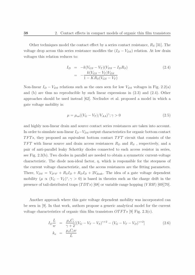
Other techniques model the contact effect by a series contact resistance, RS [31]. The
voltage drop across this series resistance modifies the (ID − VDS) relation. At low drain
voltages this relation reduces to:
ID = −k(VGS − VT )(VDS − IDRS) (2.4)
= − k(VGS − VT )VDS
1−KRS(VGS − VT )
Non-linear ID − VDS relations such as the ones seen for low VDS voltages in Fig. 2.2(a)
and (b) are thus no reproducible by such linear expressions in (2.3) and (2.4). Other
approaches should be used instead [62]. Necliudov et al. proposed a model in which a
gate voltage mobility is:
µ = µoo((VG − VT )/VAA)γ; γ > 0 (2.5)
and highly non-linear drain and source contact series resistances are taken into account.
In order to simulate non-linear ID−VDS output characteristics for organic bottom contact
TFTs, they proposed an equivalent bottom contact TFT circuit that consists of the
TFT with linear source and drain access resistances RD and RS , respectively, and a
pair of anti-parallel leaky Schottky diodes connected to each access resistor in series,
see Fig. 2.3(b). Two diodes in parallel are needed to obtain a symmetric current-voltage
characteristic. The diode non-ideal factor, η, which is responsible for the steepness of
the current voltage characteristic, and the access resistances are the fitting parameters.
There, VDS = VD′S′ + RSID + RDID + 2Vdiode. The idea of a gate voltage dependent
mobility (µ ∝ (VG − VT )γ, γ > 0) is based in theories such as the charge drift in the
presence of tail-distributed traps (TDTs) [68] or variable range hopping (V RH) [69][70].
Another approach where this gate voltage dependent mobility was incorporated can
be seen in [9]. In that work, authors propose a generic analytical model for the current
voltage characteristics of organic thin film transistors OTFTs [9] Fig. 2.3(c).
IDL
w=
µoCi
γ + 2[(VG − VT − VS)
γ+2 − (VG − VT − VD)γ+2] (2.6)
ko =µoCiw
L

2.3. DC models 39
where VG and VT are the gate bias voltage and the threshold voltage, respectively. The re-
sult is equivalent to the well known and widely used generic FET model with a constant
mobility. It is derived considering a voltage drop between the external source termi-
nal and the internal source (VS ≡ VC) and the mobility µ is written according to the
aforementioned common theoretical result [68], and [69] or [71],
µ = µo(VG − VT − Vx)γ
where Vx is the potential in the semiconducting film of the TFT .
Assuming the values of ko, γ and VT are known, a value for VC can be found from
an experimental drain current. Thus complete ID − VC curves can be extracted from
experimental output characteristics ID = ID(VG, VD). The extraction of the ID−VC cur-
ves requires the previous determination of ko, γ and VT . The authors that proposed this
generic drift model also proposed an extraction method to determine these parameters.
It consists of a several step process [72] developed on identically processed transistors
with different channel lengths (but the same channel width). It is similar to the model
with a constant mobility in (2.2). By choosing the correct value for ko, it makes all the
ID − VC curves extracted from the different transistors to coincide. Thus, the usefulness
of this extraction method is reduced to situations where several devices with different
channel lengths, but otherwise identical, are available. In any case, prior to the deter-
mination of ko, proper parameter extraction techniques are required to determine VT
and γ in (2.6)[73]. As mentioned in the introduction, the voltage drop at the contact
region seriously affects the extraction of these and other parameters. Unless there is a
method that eliminates these effects, an iterative procedure should be more convenient.
Moreover, it would be very useful to find a simple and physically based model for the
ID − VC relation at the contact in order to introduce this model in a previous generic
FET model. It should employ as few parameters as possible, in order to maintain the
compactness of the receiver generic FET model. In this chapter, we have chosen (2.6)
to incorporate the contact effects in, as it allows for an easy implementation and modi-
fication. Other details of the versatility of this model can be found in [1]. Our purpose
is that the resulting model, after the incorporation of the contact effects, has parame-
ters that can be characterized relatively easily, or even guessed, preventing unnecessary
phenomenological fitting parameters. This is done in the following sections.

40 2. Contact effects in compact models of organic thin film transistors
2.4. Contact model
For the contact region a functional model of the carrier injection VC = VC(ID),
developed in [4][36] is initially used:
VC = Vinjection(ID) + Vredox(ID) + Vdrift(ID) (2.7)
The model takes into account different physical chemical mechanisms that take place at
the contact: carrier injection through the barrier, Vinjection , ion formation at the interface
(redox reactions), Vredox , and charge drift in the low conductivity region of the organic
material at the contact, Vdrift. The expressions for the different components in (2.7)
are detailed in [63]. For low values of the energy-barrier height (cases expected in well
designed transistors), (2.7) is reduced to VC ≈ Vdrift(ID). It is shown in [36] that the
voltage drop associated with the charge drift depends on the free charge density at the
interface, p(0):
Vdrift =2
3(2J
εµθ)1
2 ([xC + xp]3
2 − [xp]3
2 )
xp ≡ Jθε
2e2µ[θp(0)]2(2.8)
where J = ID/S is the current density, ǫ is the permittivity of the organic material, µ is
the mobility of the carriers, q is the ratio of free to total charge density, xC is the length
of the contact region in the organic material, and the characteristic length xP is defined
as the point from the contact interface towards the organic film, at which the charge
density p(xp) decays to p(0)/√2. (Note: Please, be aware that the notation xp and xC
have the same meaning similar to those defined in [36]. In Ref. [4], L and xC were used
instead of xC and xp, respectively). Eq (2.8) shows two asymptotical trends [36]. If the
characteristic length xp is a few times larger than the contact length xC , Eq. (2.8) tends
to Ohm’s law:
ID ≈ qSp(0)µθVC/xC ≡ VC/RC (2.9)
A non-linear relation between the current and voltage in the drift term occurs when the
characteristic length xp is much smaller than the contact length xC and Eq. (2.8) reduces

2.4. Contact model 41
to the Mott–Gurney law [74][26]:
ID ≈ (9/8)εµθSV 2C/x
3C ≡ M × V 2
C (2.10)
These linear and quadratic behaviours are present in experimental data. An example of
this can be seen in poly (3-hexylthiophene) OTFTs with different source and drain elec-
trodes, Cr and Au, (Fig. 2 in [75]). The existence of different metallic electrodes produces
different contact voltage curves, showing these linear or non linear responses. Transitions
from linear to quadratic regimes can be seen not only by changing the electrodes but
also with the same electrode and varying the injection regime. This transition can be
seen in Fig. 3 in [76], where current voltage curves for hole injection into P3HT through
Au are represented. The inclusion of the ID − VC relations (2.9) or (2.10) in the generic
model (2.6) adds a new parameter to the model. Drawing current curves ID = ID(VD, VG)
knowing the set of parameters (VT , ko, M or R) is an easy task. However, extracting
these parameters from experimental output characteristics is a major problem. There are
well established parameter extraction techniques for FETs that can be used to extract
the parameters in (2.6). An appropriate technique is proposed in [73], by the so called
HV G function, which extracts the values of γ and threshold voltage VT from the linear
operation regime of the OTFT . The HV G function is the ratio of the integral of the drain
current over the gate bias divided by the drain current. The corresponding equation for
the HV G function derived from the TFT generic model (2.6) is:
HV G(VG) =
∫ VG
<VTIDdVG
ID(VG)
HV G(VG) =1
γ + 3
(VG − VT − VS)(γ+3) − (VG − VT − VD)
(γ+3)
(VG − VT − VS)(γ+2) − (VG − VT − VD)(γ+2)(2.11)
HV G(VG) ≈ (VG − VT )
(γ + 2)[1− R2(
VD
VG − VT
)], VD ≪ (VG − VT ) (2.12)
HV G(VG) =(VG − VT − VS)
(γ + 3), VD > (VG − VT )
where R2(VD/(VG−VT )) is the remainder term, that represents the error in approximating
HV G(VG) by the above first order power series. In these equations, as stated in [73], HV G

42 2. Contact effects in compact models of organic thin film transistors
becomes a linear function of gate overdrive (VG − VT ) by setting VS = 0, while ko is
cancelled, which is the advantage of the method. However, Eq(2.12) explicitly neglects
the effect of the contacts, as VS is assumed null. That means that the values of VT and γ
may not be correct. To check this fact a hypothetical p-type transistor with the following
parameters is considered: VT = 4.5 V, γ = 1, VS = VC = IDR, R varying in the range
(102 − 108Ω) and ko in the range (10−6 − 10−12 A/V2). The HV G function, as defined in
Eq(2.12), is built, and parameters VT and γ are determined in the saturation region as
recommended in [72].
Fig. 2.5 shows the results of this method. There are ranges of R in which the extracted
values for VT and γ differ significantly from the original ones. A direct and easy-to-
implement method like this one, in the absence of contact effects, is clearly altered
under the presence of contact effects. Contact effects can really be a bottleneck in the
extraction of the main parameter of the transistor. Despite these difficulties, we propose
an extraction method in which the advantages of these methods are considered. In the
next section, we propose a procedure to extract from experimental ID − VD curves, not
only the values of VT and γ, but also the contact voltage VS, characterized by parameters
M or R (Eqs. (2.10, 2.9) and, respectively), and the value of ko.
2.5. Parameter extraction method
Upgrading a model by the introduction of new physical effects means the incorpo-
ration of additional fitting parameters that may not be possible to adjust consistently,
or interfere with previous parameters of the model. The interference among parameters
can be eliminated by a good initial estimation of some of them. In the case of contact
effects, we provide a procedure that initially estimates the parameters associated to the
contacts by slightly modifying the ideal c−MOS model. Although the ideal c−MOS
model cannot accurately reproduce the complete output characteristics of an OTFT , it
does provide a good initial estimation of the transistor parameters to be subsequently
determined in (2.6), in particular those associated to the contacts. In this section, we
define the steps followed to determine the complete set of parameters in (2.6), including
the parameter associated to the contact region.
1. Estimation of VT and k from the ideal c−MOS model in saturation (2.1).

2.5. Parameter extraction method 43
Figure 2.5: a) Extracted µ , and b) extracted VT from the generic drift model (2.6) using theHV G method [73][72] for a transistor with initial parameters VT = 4.5 V , γ = 1 and contacteffects showing a linear behaviour VS = VC = IDRC . The extracting γ and VT representedfor transistors with different ko and R. Neglecting the voltage drop at the contact in the HV G
function makes the extracted values to differ from the original ones.

44 2. Contact effects in compact models of organic thin film transistors
2. Estimation of the electric field degradation of mobility by analysing the saturation
region of the transistor. Eq. (2.5) is introduced in (2.1) and parameters defining
the gate voltage dependent mobility are determined from the saturation region.
3. Estimation of contact parameters (curves ID − VC : ID = M(VGS)V2C or ID =
VC/R(VGS). The drain source voltage is modified in (2.1) by the inclusion of the
voltage drop at the source contact. The model is represented in Fig. 2.3(a). For the
TFT the usual analytic expression for the MOS transistor can be used:
ID = −k((VGS′ − V ′
T )VDS′ − VDS′/2) (2.13)
where VDS = VDS′ + VC and V ′
T is an internal threshold voltage defined for the
intrinsic transistor in Fig. 2.3(a). V ′
T can be evaluated as V ′
T = VT − VC(IDsat),
where VT is the threshold voltage extracted from the saturation region of the expe-
rimental data and VC(IDsat) is the average value of the contact voltage evaluated
in saturation, ID = IDsat, and different gate voltages. V ′
T is not known, as the
contact voltage is not known at this step. In a first estimation, the modification
of the gate voltage by the contact effects is neglected. It can be checked that this
simplified model can reproduce the data in the linear region, where the contact
effects are clearly dominant, by assuming (VGS′ − V ′
T ) ∼ (VGS − VT ) in Eqs. (2.13),
(2.7) and (2.9)(or (2.10)). The effect of the contact voltage on the gate voltage is
compensated by a modification of the threshold voltage for the intrinsic TFT . The
idea of the internal threshold voltage is formally introduced and physically derived
in (2.2) (or in (2.6) if the gate voltage dependent mobility is considered). In this
work, (2.13) is preferred for an initial estimation of the parameter M (or R). It
avoids the mutual interference between the contact parameter M (or R) and the
rest. It avoids the need of introducing an intrinsic threshold voltage, V ′
T , in the
OTFT model by the existence of contact effects.
4. Estimation of an average value for the contact voltage VS in the saturation region.
Once the M (or R) parameter is extracted from the experimental data (M =
M(VGS) or R = R(VGS)), the average value of the contact voltages evaluated at
ID = IDsat for different gate voltages can be determined, VS = VC(IDsat) .
5. Determination of VT and γ from the HV G function. The HV G function can be

2.5. Parameter extraction method 45
evaluated introducing this average value for VS in the saturation region:
HV G(VG) = (VG − VT − VS)/(γ + 3) (2.14)
Once the effects of the contacts are introduced in this function, VT and γ can be
determined more accurately. The problems associated to the contact effects make
the linear region no valid for the determination of such parameters. The saturation
region has previously been suggested as the most appropriate region to carry on
this characterisation [72].
6. a) Final determination of ko and M(VGS) (or R(VGS)). At this step, values for
all the variables appearing in the drift generic model (2.6) have been derived.
VT and γ have been determined by considering the contact voltage and using
a technique that eliminates the dependence with ko (see 2.11). Thus, ko and
M (or R) are the only parameters that require a final adjustment. In this
case, Eq. (2.6) is used to find these values by comparing this equation with
the experimental data. The parameter ko mainly affects the saturation region
and M (or R) affects the linear region. Thus, these parameters are modified
in order to fit the current voltage curves in these respective regions. Slight
modifications of these two parameters found this way may be necessary to
reproduce the complete set of experimental ID(VD, VG) curves.
b) Direct extraction of the ID − VC curves from (2.6). The objective of this step
is twofold: (i) as a test to check the values of the parameters obtained in step
6a or (ii) as an alternative step for 6a when non reasonable values for γ are
obtained in step 5.
(i) An inspection of Eq. (2.6) shows that with the values of the parameters
ko, VT , γ and M (or R) and the experimental ID(VD, VG) curves, one can
derive ID − VC curves at different VG. These ID − VC curves must match
the ones obtained in step 6a (controlled by Eqs (2.9) and (2.10)). Step
6b alone can be used to determine a unique ID − VC curve for several de-
vices with different channel lengths, but otherwise identical [59][60][61],
as mentioned in the previous section. All the extracted curves must con-
verge into one. However, step 6b alone cannot be employed for the case

46 2. Contact effects in compact models of organic thin film transistors
of a set of single lengths transistors, as convergence is not guaranteed.
Steps 1-5 provide such a procedure towards a convergence, towards the
physical trend given by Eqs. (2.9) and (2.10). In any case, the extraction
of different ID − VC curves for different values of ko, and its comparison
with the value of ko and the curves extracted in step 6a are suggested.
(ii) The other situation where this step is necessary is when abnormal values
of γ or VT are obtained in previous steps, despite introducing an estimated
value for the contact voltage VS. A negative value of γ clearly indicates
that the characterization needs further processing (see Fig. 2.5(a)). In
these situations, convergence in Step 6a is not achieved. An iterative
procedure is suggested in this step 6b. The initial values used for γ, VT
and ko in this procedure depend on the value of γ estimated in previous
steps. The value of the threshold voltage is assumed initially correct.
In case the value of γ extracted from step 2 is positive, this should be
assumed as an initial estimation. On the contrary, the initial value for γ
is assumed zero. For the selected value of γ, ko is varied until a physical
result for the ID − VC curves is obtained. If it does not exist the value
of γ is increased and ko is again modified. The values of γ and ko are
alternatively modified until the ID−VC curves behave like (2.9) or (2.10).
An arbitrary set of values for VT , γ and ko, different from the actual
solution, produces current voltage curves at the contact with no physical
meaning (such as a change of the sign of the contact voltage or strange
trends in the ID−VC curves). In case, the extracted ID−VD curves provide
a value of VS = VC(IDsat) different from the one initially estimated in step
5, a new iteration is necessary. A new value for the threshold voltage would
be determined in step 5 and step 6b would be repeated.
2.6. Application to experimental results
To check the validity of the extraction method for the contact voltage drop and the
rest of the basic parameters appearing in the TFT generic model (2.6), we analyse data
showing both linear and non-linear effects. We analyse measured ID−VD curves in ZnPc-
based organic thin film transistors and data taken from other authors’ experiments.

2.6. Application to experimental results 47
2.6.1. Non-linear contact current-voltage curves
Experimental data on ZnPc based transistors.
In first place, we analyse the experimental data depicted in symbols in Fig. 2.2(a)and
(b). They show a clear non-linear behaviour at low drain voltages pointing out the
existence of contact effects. Considering the values of the HOMO and LUMO levels for
the organic film and the electrode work function given above, the energy barrier of the
Au− ZnPc contact can be considered small enough to prevent current to flow through
it. The current is thus dominated by the drift term. Due to the high non-linearity of the
ID − VD curves, the current-voltage relation at the contact is modelled by (2.10). The
extraction procedure detailed in the previous section can be followed in Fig. 2.6.
We initially consider that the values of the mobility (assumed gate voltage dependent)
and threshold voltage are extracted by fitting the experimental data in the saturation
region with the ideal c−MOS model: VT = −2.52 V, γ = −0.0224, VAA = 24.4 V and
µoo = 1.8 × 10⁻⁶ cm2/Vs for the transistor of Fig. 2.2(a) and VT = −1.7 V, γ = −0.03,
VAA = 24.4 V and µoo = 4.4×10⁻⁶ cm2/Vs for the trnasistor of Fig. 2.2(b). The result of
these fitting (steps 1 and 2) can be seen in Fig. 2.2(a) and (b). If the contact effects are
introduced in the ideal MOS model (step 3) a good agreement between the experimental
data (symbols) and the combined expression resulting from (2.10) and (2.13) (solid lines)
is seen in: Fig. 2.6. The values of M introduced in (2.10) to achieve such an agreement are
M =(1.2, 1.5, 1.66, 5.0, 1.5)×10−10 A/V2 for VGS =0, 10, 20, 30 and 40 V, respectively,
for the transistor of Fig. 2.6(a), and M =(1.0, 1.2, 1.2, 4.0, 9.5)×10−10 A/V2 for VGS =0,
10, 20, 30 and 40 V, respectively, for the transistor of Fig. 2.6(b). The contact ID − VC
curves resulting from these parameters are depicted in dashed lines on the right region
of Fig. 2.6(a) and (b). Once we know these curves, the contact voltage can be evaluated
in the saturation region for each gate voltage. These points are marked with the tips of
the dashed arrows in Fig. 2.6(a) and (b). An average value VS(average) ≈ −3 V and -4
V for Fig. 2.6(a) and Fig. 2.6(b), respectively, are obtained from these points (step 4).
The fifth step corresponds to the determination of VT and γ from the HV G function,
once a value for the contact voltage in the saturation region has been estimated. The
analysis of the HV G function provides the following values: (γ = 1.026 and VT = 10.51
V) and (γ = 0.8 and VT = 13 V) for the transistors in Fig. 2.7(a) and (b), respectively.
Very different values for the threshold voltage are obtained in comparison to the ones
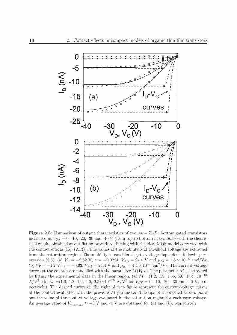
48 2. Contact effects in compact models of organic thin film transistors
Figure 2.6: Comparison of output characteristics of two Au−ZnPc bottom gated transistorsmeasured at VGS = 0, -10, -20, -30 and -40 V (from top to bottom in symbols) with the theore-tical results obtained at our fitting procedure. Fitting with the ideal MOS model corrected withthe contact effects (Eq. (2.13)). The values of the mobility and threshold voltage are extractedfrom the saturation region. The mobility is considered gate voltage dependent, following ex-pression (2.5); (a) VT = −2.52 V, γ = −0.0224, VAA = 24.4 V and µoo = 1.8 × 10⁻⁶ cm2/Vs;(b) VT = −1.7 V, γ = −0.03, VAA = 24.4 V and µoo = 4.4× 10⁻⁶ cm2/Vs. The current-voltagecurves at the contact are modelled with the parameter M(VGS). The parameter M is extractedby fitting the experimental data in the linear region; (a) M =(1.2, 1.5, 1.66, 5.0, 1.5)×10−10
A/V2; (b) M =(1.0, 1.2, 1.2, 4.0, 9.5)×10−10 A/V2 for VGS = 0, -10, -20, -30 and -40 V, res-pectively). The dashed curves on the right of each figure represent the current-voltage curvesat the contact evaluated with the previous M parameter. The tips of the dashed arrows pointout the value of the contact voltage evaluated in the saturation region for each gate voltage.An average value of VSaverage ≈ −3 V and -4 V are obtained for (a) and (b), respectively
.

2.6. Application to experimental results 49
Figure 2.7: Comparison of output characteristics of an Au − ZnPc bottom gated transistormeasured at VGS = 0, -10, -20, -30 and -40 V (from top to bottom in symbols) with thetheoretical results obtained at our fitting procedure. Fitting with the generic drift model (2.6).This equation is evaluated with the following parameters. Parameters VT and γ are determinedwith theHV G function (2.12) including the contact effects VS = VSaverage (γ = 1.026, VT = 10.51V, γ = 0.8, VT = 13 V for a and b, respectively); the value of µo is the one calculated from thesaturation region with the ideal MOS model (µo = 1.8× 10⁻⁶ and 4.4× 10⁻⁶ cm2/Vs for a andb, respectively); and VS = 0. The last two parameters make the theoretical result to disagreewith the experimental curves.

50 2. Contact effects in compact models of organic thin film transistors
extracted in step 1. Figs. 2.7(a) and (b) illustrate the comparison of the experimental
data with the generic drift model (2.6) using the values of these last two parameters,
the value of µo determined from the saturation region with the ideal c − MOS model
(µo = 1.8 × 10⁻⁶ for Fig. 2.7(a)) and (4.4 × 10⁻⁶ cm2/Vs for Fig. 2.7 (b)), and VS = 0.
It is apparent that the mixture of values of parameters extracted from different models
and ignoring the contact effects produce such a disagreement.
A change of the value of the mobility to 1.8 × 10⁻⁷ cm2/Vs and 1.7 × 10⁻⁷ cm2/Vs
for Figs. 2.8(a) and (b), respectively is necessary in order to fit the experiments in the
saturation region (Fig. 2.8(a) and (b)). In these figures, VS is maintained null in order to
highlight this fact. Finally, the contact effects, by means of the parameterM in (2.10), are
introduced in the generic drift model (2.13). The combined model fits the experimental
data for the following set of values: M =(0.2, 0.8, 1.42, 3.32, 4.02)×10−10 A/V2 in Fig.
2.9(a), and M =(0.3, 10, 0.7, 1.2, 5.0, 9.5)×10−10 A/V2 in Fig. 2.9(b) for VGS =0, -10,
-20, -30 and -40 V, respectively. A unique value for M should be expected for a compact
model. However, the compactness of this parameter is justified below by its relation with
the charge density in the intrinsic channel.
The analysis of the values of the different parameters extracted in the six steps shows
that the variations in VT and γ (from the initial estimations to the final results) are very
significant, while the parameterM is practically unaffected by when using either the ideal
c−MOS model or the generic drift model, both in combination with our contact model.
On the one hand, the generic drift model is physically well based. However, the inclusion
of new parameters in it makes their extraction more difficult. On the other hand, the use
of simple models like the one propose in (2.13), although based on approximations, are
really helpful in finding a proper initial estimation of the contact ID − VC curves. This
is necessary to proceed with the determination of the exact values of the parameters
appearing in (2.6).
The current-voltage curves at the contact can be directly extracted from (2.6) once
the parameters µo, γ and VT are known [72]. These curves, for the as-deposited ZnPc
transistor of Fig. 2.2(b), can be seen with symbols in Fig. 2.10. The values of these para-
meters correspond to the ones extracted with our procedure in the previous paragraphs.
The inset of Fig. 2.10 shows the comparison of the experimental data with (2.6) inclu-
ding these current voltage curves. The agreement is clearly better than the one shown in
Fig. 2.9(b). However, the current voltages curves extracted with our procedure (shown

2.6. Application to experimental results 51
Figure 2.8: Comparison of output characteristics of an Au − ZnPc bottom gated transistormeasured at VGS = 0, -10, -20, -30 and -40 V (from top to bottom in symbols) with thetheoretical results obtained at different steps of our fitting procedure. Fitting with the genericdrift model (2.6) changing the parameter µo to 1.78× 10⁻⁷ cm2/Vs and 1.7× 10⁻⁷ cm2/Vs fora and b, respectively; VS is maintained null.

52 2. Contact effects in compact models of organic thin film transistors
Figure 2.9: Comparison of output characteristics of an Au − ZnPc bottom gated transistormeasured at VGS = 0, -10, -20, -30 and -40 V (from top to bottom in symbols) with the theo-retical results obtained at different steps of our fitting procedure. Fitting with the generic driftmodel (2.6) introducing the contact effects. µo does not change. The extracted M parameterare: a)M=(0.5, 0.8, 1.4, 2.52, 4.029)×10−10 A/V2 and b) M=(0.3, 0.7, 1.2, 5.0, 9.5)×10−10
A/V2 for VGS = 0, -10, -20, -30 and -40 V, respectively. Despite the large modification of thevalues of VT and µo along the different steps of this procedure, the values of the parameter Massociated to the contact voltage suffer almost no variation. That means that the use of singlemodels, like the one propose in (2.13), helps finding a proper estimation of the contact ID−VD
curves.

2.6. Application to experimental results 53
Figure 2.10: Current voltage curves at the contact extracted from the experimental outputcharacteristics of the as-deposited ZnPc transistor of Fig. 2.2(b) at different gate voltages withour procedure (solid lines) and directly from the generic drift model (2.6) (symbols). Theparameters employed in the calculation correspond to the final ones obtained in 2.6. Inset:Comparison of output characteristics of an Au − ZnPc bottom gated transistor measured atVGS =0, -10, -20, -30 and -40 V (from top to bottom in symbols) with the theoretical resultsfrom (2.6) using the ID − VC curves shown in symbols in the main Figure.
as solid lines in Fig. 2.10) provide a physical trend and a way to interpret the ones shown
as symbols.
Analysis of other experimental data.
Experimental data measured in an Au-pentacene BC − TFT by other authors [62]
are also reproduced by our model. Fig. 2.11 shows a comparison of the experimental data
(symbols) with the generic drift model (2.6) in which the contact current-voltage relation
(2.10) has been incorporated (solid lines). The transistor has the following characteristics:
the SiO2 gate-dielectric thickness is tox = 290nm, the gate length is L = 20 µm and the
gate width w = 220 µm.
The model parameters have been extracted using the procedure detailed in the pre-
vious section. This is a case where the value of γ extracted in step 5 shows an abnormal

54 2. Contact effects in compact models of organic thin film transistors
Figure 2.11: a) Comparison of output characteristics of an Au-Pentacene bottom gated tran-sistor at VGS =0, -10, -20, -30, -40, -50 and -60 V from top to bottom (symbols) with the genericdrift model (2.6) including non-linear contact effects (2.10) (solid lines). The dimensions of thetransistor are tox = 290×10−7 cm, w = 220×10−4 cm, L = 20×10−4 cm. The parameters usedin the model, determined according to the method detailed in this work, are k = 7.78 × 10⁻⁸
A/V2, µo = 0.19 cm2/Vs, VT = 17.3 V, γ = 0.118, M =(0.5, 0.8, 1.0, 1.5, 2.0, 2.4, 2.5)×10−6
A/V2 for VGS = 0, -10, -20, -30, -40, -50 and -60 V, respectively. b) Normalized values of thecharge density in the channel, ρ, and free to total charge density ratio θ in the low conductivityregion near the contact. The values of θ are extracted from the previous values of M and itsdefinition in (2.6). The normalization values are: ρmax = 3.4 × 1018 cm−3 and θmax = 0.06.The charge densities in the channel and in the contact region are correlated meaning that thevalues of M extracted by our procedure are acceptable.

2.6. Application to experimental results 55
value despite including the contact effects, γ = −0.4. In this situation, step 6b was fo-
llowed instead of step 6a. The value of γ extracted by analysing the saturation region
with the ideal c −MOS model (2.1) in combination with the electric field degradation
of the mobility (2.5) was used instead, γ= 0.118. The value of the threshold voltage was
determined in step 5 by means of the HV G function applied to the generic drift model
(2.6). The parameters obtained after the fitting procedure are: ko = 7.78 × 10⁻⁸ A/V2,
µo = 0.19 cm2/Vs, VT = 17.3 V, γ = 0.118, M =(0.5, 0.8, 1.0, 1.5, 2.0, 2.4, 2.5)×10−6
A/V2 for VGS = 0, -10, -20, -30, -40, -50, -60 V, respectively. Situations analysed in Fig.
2.6 and Fig. 2.11 shows the need to employ the advantages of simple models (although
not exact ones) and to combine them in a precise sequence. The objective is to determine
correct values for the transistor parameters that appear in a more compact and precise
model, such as the one in (2.6).
Another feature of our model and its associated extraction procedure is that they
allow us to determine the parameter M defined in (2.10). From this parameter, we
can determine the evolution of the free to total charge-density ratio θ, with the gate
voltage. Assuming the same value for the mobility in the transistor channel and in the
low conductivity region at the contact, this ratio varies from 0.012 at VGS = 0 V to 0.060
at VGS = −60 V . The values of θ, necessary to fit the experimental data with our model
(Fig. 2.11(a)), are represented as a function of the gate voltage in Fig. 2.11(b) (circles).
In this figure, we also represent the values of the charge density in the intrinsic channel,
estimated according to the equation (solid line) [77],
ρchannel = Ci(VG − VT )/to (2.15)
where to is the thickness of the organic material.
The evolution of the ratio of free to total charge density with the gate voltage is
in excellent agreement with the evolution of the charge density in the channel. This
agreement validates the physical model we propose for the DC characteristics of organic
TFTs affected by contact effects.
The non-linear behaviour shown at low drain voltages in the experiments of Fig. 2.6
and Fig. 2.11 can also be reproduced by diodes in series with a resistance connected at
the source and drain terminals (Fig. 2.3(b)). Good agreements between the experimental
data and this model are obtained. For the experimental data in Fig. 2.6, the values of the

56 2. Contact effects in compact models of organic thin film transistors
model parameters in Fig. 2.3(b) that achieve the best fit are γ = −0.032, µo = 2.65×10⁻⁴
cm2/Vs, VAA = 25.0 V, RD,S = 104 Ω, energy barrier at the interface φB = 0.65 eV and
non-ideality factor of the diode η = 5. For the experimental data in Fig. 2.11, the values
of the model parameters that achieve the best fit are γ = 0.118, µo = 0.2 cm2/Vs,
mobility evaluated at VGS = −60 V, µ = 0.27 cm2/Vs, VAA = 5.70 V, RD,S = 5 kΩ,
energy barrier at the interface φB = 0.65 eV and non-ideal factor of the diode η = 2.5.
Although the model in Fig. 2.3(b) can reproduce the experimental data, the values of
the resulting parameters should be analysed with care, especially when high values of the
non-ideal factor of the diodes and/or negative values of γ are extracted. The advantage
of our model (Fig. 2.3(c)) is its physical approach to the real mechanisms affecting the
low conductivity region near the contacts [35][4].
2.6.2. Linear contact current-voltage curves
Current-voltage ID − VD curves showing linear responses at low drain voltages have
also been studied in this work. Here, we apply the procedure from the previous section
to extract the mobility, threshold voltage and the contact voltage drop from the output
characteristics of poly(3 − hexadecylthiophene)(P3HDT ) transistors [36] (symbols in
Fig. 2.12(a)). The solid lines correspond to the evaluation of the generic drift model
(2.6) in which the linear contact voltage-current model in (2.9) has been incorporated.
The values of the contact resistances R = R(VG) and the rest of the model parameters
are detailed in the same figure. A good agreement is observed between the experiments
and the theoretical results. The extraction procedure followed with these data does not
end in step 6a, but goes through step 6b. This is another example where the parameter γ
is clearly affected by the contact effects (see Fig. 2.5). In step 5, γ = −0.3 and VT = −4.5
V are obtained assuming an average value for the contact voltage in the saturation region
VS = VC(IDsat) = −1.5 V. The value of γ is gradually increased and the value of ko is
modified until the extracted ID−VC curves show a perfectly linear behaviour, as expected
by the trend of the experimental data at low drain voltages. This occurs for γ = 1.5 (Fig.
2.12(b)). The value of the threshold voltage needs no modification.
In order to check, that this solution is unique, other pairs of values for γ and ko
are tested. As an example, Fig. 2.13 shows ID − VC curves extracted from (2.6) for a
lower γ, γ = 0.15, VT = −4.5 V and different values of ko, after equating ID, VG and

2.6. Application to experimental results 57
Figure 2.12: a) Output characteristics of an Au−P3HDT BC transistor at VG = -8, -10, -12,-14, -16, and -18 V from the top to the bottom. Symbols represent the experimental data [67]based on material described in [78][79]. Lines represent the fitting with the with the genericdrift model (2.6) including linear contact effects (2.9). The details of the samples are: thermallygrown SiO2 (∼ 200 nm), channel width w = 0.5 cm (multi-finger configuration), and channellength L = 10 µm. The polymer film is 7 nm thick and was deposited by spin coating. Theparameters used in the model, determined according to the method detailed in this work, areko = 3×10⁻⁸ A/V2, µo = 1.2×10⁻⁵ cm2/Vs, VT = −4.5 V, γ = 1.5, R =(4.9 , 4.8, 4.7, 4.6, 4.5,4.0)×107 Ω for VG = -8, -10, -12, -14, -16, and -18 V, respectively. b) Current voltage curvesat the contact extracted from the experimental output characteristics at different gate voltageswith our procedure (solid lines). The parameters employed in the calculation correspond to thefinal ones obtained in Fig. 2.12(a). The current voltage curves at the contact extracted directlyfrom the generic drift model (2.6) are shown in symbols.

58 2. Contact effects in compact models of organic thin film transistors
Figure 2.13: Contact current-voltage curves extracted from the experimental data of Fig. 2.12,directly from Eq. (2.6) (symbols) providing this model with the parameter values VT = −4.5V and γ and ko given in the figures. The solid lines are used as a reference. They correspond tothe final results obtained with our procedure for the ID−VC curves (Fig. 2.12). No convergenceto a physical acceptable solution is seen when varying the parameter ko for γ = 0.15: figures(a) to (d). A similar lack of convergence towards a physical acceptable trend for the ID − VC
curves is seen for other values of γ, except for the actual solution depicted in Fig. 2.12
VD to the experimental data (symbols). They are compared to the solution obtained
in Fig. 2.12(b). The set of figures shows that there is no acceptable ID − VC curve in
any case. Fig. 2.13(a) shows positive values for VC when negative ones are expected.
Figs. 2.13(b)-(d) show linear responses at low values of VC . However, the curves tend
to saturate, reflecting the saturation response of the intrinsic channel, not the actual
response of the contact region. A similar study was made with different values of γ,
showing that the solution depicted in Fig. 2.12 is unique. As seen in these two sub-
sections, the model distinguishes between linear responses and quadratic responses for

2.6. Application to experimental results 59
Figure 2.14: Measured output ID − VDS characteristic in a Cr/P3HT/Cr OTFT [75](solidline). It is shown with the extracted ID − VC curve (squares) and the three components of Eq.(2.7) [63], Vred (circles), Vdrift (triangles), and Vinjection (dashed line).
the current voltage relation at the contact region. Both responses are included under
the assumption that the energy barrier at the contact imposes no restriction to the
current, i.e. under the assumption of space charge limited transport . Therefore, the
model is limited to these situations. Outside these limits, when the energy barrier at the
interface imposes a restriction to the current, non linear I−V responses are also obtained,
however not necessarily quadratic ones (thermionic emission or tunnel injection should
be considered (2.7)). An example of this can be seen in Fig. 2.14, where the voltage
drop at the contact of an OTFT is the sum of the voltage drop at the space charge
region and the voltage necessary to surpass the barrier at the contact (a combination of
injection through the barrier and space charge transport). For these cases, the quadratic
model can still be used by taking into account that we are working under a second order
approximation, and no connection with the physical parameters appearing in (2.10) is
possible. In any case, properly designed transistors are expected to use contacts with low
energy barriers at the interface in order to reduce the injection-voltage term. Therefore,
from this practical point of view, the model can be consider of full applicability.

60 2. Contact effects in compact models of organic thin film transistors

3
Test of the extraction method
3.1. Introduction . . . . . . . . . . . . . . . . . . . . . . . . . . . . 62
3.2. Test of the method . . . . . . . . . . . . . . . . . . . . . . . . 63
61

62 3. Test of the extraction method
Figure 3.1: Proposed equivalent circuit of a TFT including the voltage drop at the sourcecontact, VC ≈ VS .
3.1. Introduction
The objective of this chapter is to test the procedure developed in Chapter 2 by
applying it to output characteristics of a transistor with known parameters. The tran-
sistor under test is represented in Fig. 3.1. It consists of an ideal transistor plus contact
effects where VDS = VD − VS. The output characteristics are modelled by:
IDL
w=
µoCi
γ + 2[(VG − VT − VS)
γ+2 − (VG − VT − VD)γ+2] (3.1)
ID = MV 2S ,M =
9
8θεµS
(xc)3(3.2)
We consider a p-type OTFT with the following parameters: µo = 5.0× 10⁻⁷ cm2/Vs
, γ = 0.0, VT = −2.5 V, L = 5 µm, w = 10 mm, Ci = 20.7 nF we consider non linear
contact effects modelled with the parameter M , and the following dependence with the
gate voltage: M(VGS) = 10−11 − 3.5× 10⁻¹² × VG(A/V2). The resulting ID − VD curves
for different VG are represented with symbols in Fig. 3.2. Our objective is to show that
our method is able to recover the value of these parameters from these curves. We only
assume as known parameters those associated to the geometry of the device (L, w, Ci).

3.2. Test of the method 63
−20 −15 −10 −5 0−1.8
−1.6
−1.4
−1.2
−1
−0.8
−0.6
−0.4
−0.2
0
VD
(V)
I D (
nA)
Figure 3.2: ID − VD curves at VG = -6.836, -8.533, -10.173, -11.770, -13.331, -14.797, -16.306,-17.795, -19.265 and -20.721 V, from top to bottom. These curves are calculated with thecombination of (3.1) and (3.2) and the parameters defined in the text.
3.2. Test of the method
(i) In first place, we extract the value of µo and VT from the ID − VD curves in the
saturation regime by using
ID =wµoCi
L(VG − VT )VD − (
V 2D
2); VD ≤ (VG − VT ) (3.3)
ID =wµoCi
2L(VG − VT )
2;VD ≥ (VG − VT )
k =wµoCi
L
Ci =εiti
The result is µo = 2.7× 10⁻⁷ cm2/Vs, and VT = −3.4 V, clearly differing from the
original ones, in particular the threshold voltage.
(ii) The second step consists of extracting the contact voltage from these curves. We
combine the relation VD = VDS − VC (Fig. 3.1) with (3.2) and (3.3), and compare
the result with the output characteristics. To determine the relation of the drain

64 3. Test of the extraction method
−20 −15 −10 −5 0−1.8
−1.6
−1.4
−1.2
−1
−0.8
−0.6
−0.4
−0.2
0
VD
(V), VC
(V)
I D (
nA)
(ID
−VD
) (ID
−VC
)
Figure 3.3: Left hand side: Comparison between the experimental curves of Fig. 3.2 (dottedlines on the left) and theoretical ID − VD curves (solid lines) at VG = -6.836, -8.533, -10.173,-11.770, -13.331, -14.797, -16.306, -17.795, -19.265 and -20.721 V, from top to bottom. Theexperimental data are assumed to be those of an ideal transistor with contact effects as shownin Fig.3.1. The theoretical ones correspond to the combination of (3.2 ) and (3.3), i.e. neglectingthe effect of the contact voltage on VG (VG ≈ VGS). Right hand side: ID − VC curves necessaryto produce the best fitting between the experimental and theoretical ID − VD curves. Theparameters M associated to the ID − VC curves are shown in the Table 3.1. The horizontaldashed lines indicate the value of the voltage drop at the contact in saturation
voltage with the contact voltage, we estimate the value of M parameters by an
iterative procedure. The best agreement is shown in solid lines on the left, in Fig.
3.3. The resulting values of the M parameter are shown in the Table 3.1. The
ID − VC curves are shown in dotted lines on the right of Fig. 3.3. From the dotted
lines in Fig. 3.3 , we can determine the value of VC in the saturation region for
different VGS, VC (IDsaturation). Their average value is VCaverage
= −1.83 V.
(iii) In a third step, we evaluate the HV G function by integrating the drain current in
the saturation regime from the output characteristics:
HV G(VG) =
∫ VG
<VTIDdVG
ID(VG)
HV G(VG) =1
γ + 3
(VG − VT − VS)(γ+3) − (VG − VT − VD)
(γ+3)
(VG − VT − VS)(γ+2) − (VG − VT − VD)(γ+2)(3.4)

3.2. Test of the method 65
In the saturation region, the HV G function reduces to
HV G(VG) =(VG − VT − VS)
(γ + 3), VD > (VG − VT ) (3.5)
Thus we can we can determine the values of γ and VT , by assuming VS = VCaveragein
(Eq-6.12). The resulting values are γ = −0.14 and VT = −2.52 V. The value of the
threshold voltage is clearly in agreement with the final result (only an error around
0.8% is obtained). That means that the assumption made for VS is appropriate.
However, a lower value than expected is obtained for γ. When experimental data
are analysed we cannot know whether this result is correct or not. Therefore, a
next step is required.
(iv) Assuming this value of γ as correct, we proceed to determine the value of the
mobility and M parameters. We use (3.1) and (3.2) to represent ID−VD curves and
we compare them with the experimental output characteristics. We know γ and VT
from step (iii). The values of parameters µ and M can be initially considered as the
ones obtained in steps (i) and (ii), respectively. These two parameters are iteratively
modified until a good fitting is obtained between the theoretical and experimental
data (solid lines and symbols, respectively, in Fig. 3.4(a). The resulting values are
µ = 5.8× 10⁻⁷ cm2/Vs and M is given in Table. 3.2.
(v) Once the value of µo is determined, we can introduce it in (3.1) and obtain the
Table 3.1: Extracted values after step (ii) of MFS and MBS for the OTFT with outputcharacteristics in Fig. 3.3.
VG (Volts) M (A/V2)-6.836 50× 10−12
-8.533 70× 10−12
-10.173 80× 10−12
-11.770 100× 10−12
-13.331 150× 10−12
-14.797 200× 10−12
-16.306 250× 10−12
-17.795 290× 10−12
-19.265 390× 10−12
-20.721 400× 10−12

66 3. Test of the extraction method
Table 3.2: Extracted values of MFS and MBS after step (iv) for the OTFT with outputcharacteristics in Fig. 3.4(a).
VG (Volts) M (A/V2)-6.836 330× 10−13
-8.533 380× 10−13
-10.173 420× 10−13
-11.770 480× 10−13
-13.331 550× 10−13
-14.797 600× 10−13
-16.306 700× 10−13
-17.795 820× 10−13
-19.265 930× 10−13
-20.721 1030× 10−13
−20 −15 −10 −5 0−1.8
−1.6
−1.4
−1.2
−1
−0.8
−0.6
−0.4
−0.2
0
VD
(V)
I D (
nA)
−6 −4 −2 0−1.8
−1.6
−1.4
−1.2
−1
−0.8
−0.6
−0.4
−0.2
0
VC
(V)
I D (
nA)
(b)(a)
Figure 3.4: a) Comparison between experimental (x) and theoretical ID−VD curves calculatedwith the generic drift model (3.1) (solid lines). VT = −2.52 V, γ = −0.14 and µo and M areiteratively modified until a good agreement is obtained: µo = 5.8 × 10⁻⁷ cm2/Vs and M is inthe Table 3.2. VG is the same as in Fig. 3.2(b)): ID − VC curves extracted from (3.1) with thevalues of the parameters used in (a).

3.2. Test of the method 67
relation ID − VC for different gate voltages (Fig. 3.4(b)). We now proceed to test
the solution. We expect a quadratic evolution of the drain current with the contact
voltage, as seen in (3.2). That means that the slope should always increase when
|VC | increases. In Fig. 3.4(b), we see that at high values of |VC| the slope starts
decreasing and the ID−VC curves turn in a clockwise direction, deviating from the
physically expected behaviour.
(vi) To obtain a good physical behaviour for ID −VC curves, the value of γ is modified.
Lower values produce the same non-physical behaviour in the resulting ID − VC
curves as in Fig. 3.4(b). A higher value than expected one is also tested, γ = 0.29.
The new value of µo to obtain a good fitting between experimental and numerical
results (Fig. 3.5(a)) is µo = 2.9× 10⁻⁷ cm2/Vs. The ID − VC curves are extracted
from (3.1) with the values of these parameters. In this case, the slope of the ID−VC
curves goes to infinity and then decreases at high values of |VC | (Fig. 3.5(b)). TheID − VC curves turn in a counter-clockwise direction, again deviating from the
physically expected behaviour.
Table 3.3: Extracted values of MFS and MBS for the OTFT with output characteristics inFig. 3.5.
VG (Volts) M (A/V2)-6.836 478× 10−13
-8.533 488× 10−13
-10.173 498× 10−13
-11.770 508× 10−13
-13.331 518× 10−13
-14.797 528× 10−13
-16.306 538× 10−13
-17.795 548× 10−13
-19.265 558× 10−13
-20.721 568× 10−13
The value of γ is iteratively modified until the slope in the ID − VC curves always
increases with |VC |. In this case, this value is modified between -0.14 and 0.29. The
solution is archived for γ = 0, as expected. The value of the mobility for the best fitting
between experimental and numerical data (Fig. 3.6(a)) is µo = 4.8× 10⁻⁷ cm2/Vs. This

68 3. Test of the extraction method
−20 −15 −10 −5 0−1.8
−1.6
−1.4
−1.2
−1
−0.8
−0.6
−0.4
−0.2
0
VD
(V)
I D (
nA)
−6 −4 −2 0−1.8
−1.6
−1.4
−1.2
−1
−0.8
−0.6
−0.4
−0.2
0
VC
(V)
I D (
nA)
(b)(a)
Figure 3.5: Comparison between experimental (x) and theoretical ID − VD curves calculatedwith the generic drift model (3.1) (solid lines). VT = −2.52 V, γ = 0.29 and µo and M areiteratively modified until a good agreement is obtained: µo = 2.9 × 10⁻⁷ cm2/Vs and M is inthe Table. 3.2. VG is the same as in Fig. 3.2(b)): ID − VC curves extracted from (3.1) with thevalues of the parameters used in (a).
value differs only a 4% in relation to the original one. In Fig. 3.6(b), we show the
extracted ID − VC curves from (3.1) by using these last values for γ and µo. In this case,
the curves follow the trend expected in (3.2). Thus, we can conclude that the test to our
method is positive.
Table 3.4: Extracted values of MFS and MBS for the OTFT with output characteristics inFig. 3.6.
VG (Volts) M (A/V2)-6.836 350× 10−13
-8.533 390× 10−13
-10.173 430× 10−13
-11.770 470× 10−13
-13.331 510× 10−13
-14.797 550× 10−13
-16.306 590× 10−13
-17.795 630× 10−13
-19.265 670× 10−13
-20.721 710× 10−13

3.2. Test of the method 69
−20 −15 −10 −5 0−1.8
−1.6
−1.4
−1.2
−1
−0.8
−0.6
−0.4
−0.2
0
VD
(V)
I D (
nA)
−6 −4 −2 0−1.8
−1.6
−1.4
−1.2
−1
−0.8
−0.6
−0.4
−0.2
0
VC
(V)
I D (
nA)
(b)(a)
Figure 3.6: Comparison between experimental (x) and theoretical ID − VD curves calculatedwith the generic drift model (3.1) (solid lines). VT = −2.52 V, γ = 0 and µo and M areiteratively modified until a good agreement is obtained: µo = 4.7 × 10⁻⁷ cm2/Vs and M is inthe Table 3.4. VG is the same as in Fig. 3.2(b)): ID − VC curves extracted from (3.1) with thevalues of the parameters used in a).

70 3. Test of the extraction method

4
Characterization of OTFTs with
hysteresis and contact effects
4.1. Introduction . . . . . . . . . . . . . . . . . . . . . . . . . . . . 72
4.2. Variation of trapped charge during hysteresis . . . . . . . . 73
4.3. Parameter extraction from (ID − VD) curves . . . . . . . . . 74
4.3.1. Characterization method . . . . . . . . . . . . . . . . . . . . . 74
4.3.2. Trapped charge analysis of the intrinsic transistor . . . . . . . 77
4.3.3. Trapped charge analysis of the contact region . . . . . . . . . . 78
4.4. Results and Discussion . . . . . . . . . . . . . . . . . . . . . . 81
4.4.1. Non-linear contact current-voltage curves . . . . . . . . . . . . 81
4.4.2. Linear contact current-voltage curves . . . . . . . . . . . . . . . 84
71

72 4. Characterization of OTFTs with hysteresis and contact effects
4.1. Introduction
Trapping and de-trapping mechanisms can cause instabilities that produce changes in
the threshold voltage of organic thin film transistors [1][10][80]. They are also the origin of
hysteresis in current-voltage curves. The study of the hysteresis is important as it can pro-
vide information about the trapped charge in the organic material [10][45][48][50][81][82].
Subsequently, this information can be related to technological parameters with the objec-
tive of finding a better device design. Another problem that deteriorates the performance
of the organic devices is the effect of the contacts. Part of the voltage applied in these
devices is lost in the contact regions [83][84]. There are works devoted to control the
barrier of the contact. The use of self-assembled monolayers is extended to achieve this
objective [85].
In addition to controlling the barrier at the contacts, we have seen in the previous
chapters that appropriate characterization techniques are necessary to determine how
the contact region affects the electrical behaviour of the device. The combination of both
hysteresis phenomenon and contact effects makes this characterization task more difficult.
There are some previous studies that characterize the hysteresis in organic transistors
from transfer and output characteristics. In some cases, contact effects are not considered
[13]. In other cases, contact effects are eliminated from the experimental data by using
techniques, like the four-terminal method, instead of the usual two-terminal one [14].
In this chapter, we propose a method to extract information on the traps influence
on the hysteresis mechanisms in current voltage curves obtained with the two-terminal
procedure. Moreover, the proposed method solves the difficulty of processing these cur-
ves when contact effects are present. The basis underlying this method is the compact
model presented in the previous chapters [83][86]. In this part of the work, we analyse
experimental current voltage curves taken from the literature that show both contact
effects and hysteresis [13][14][87]. The characterization method based on this compact
model is applied to these data and information is extracted for the trapped charge in the
organic material. The results are compared with other values reported in the literature.
The accuracy of our method is checked by comparing our results with the ones obtained
from transient measurements [13] or the four-terminal method [14], which also considers
the contact effects.

4.2. Variation of trapped charge during hysteresis 73
Figure 4.1: Proposed equivalent circuit of a TFT including a voltage drop at the sourcecontact VC ≡ VS [86].
4.2. Variation of trapped charge during hysteresis
The hysteresis phenomenon appears in output (ID − VD ) and in transfer (ID − VG)
curves of OTFTs. In case no contact effects are present (VC = 0, VGS = VG, VDS = VD,
see Fig. 4.1), a way to know the variation of trapped charge is by measuring the difference
in drain current between forward (FS) and backward sweep (BS) curves, at certain
values of the drain and gate voltagesID(VDS , VGS) =ID(VD, VG), whereas an injection
of holes occurs in FS current and the extraction of holes occurs in the BS current [13].
The relation between the variation of the trapped charge P in the intrinsic channel of
a transistor and the current displacement ID(VDS , VGS) is given by [13]:
∆P =∆ID(VDS, VGS)× L
q × w × VDS × µ(4.1)
where q is the elementary charge, µ is the charge carrier mobility, L and w are the channel
length and width of the transistor’s organic material, respectively. In case contact effects
are present (VC 6= 0, VGS 6= VG, VDS 6= VD, see Fig. 4.1), the voltage drop at the contact
must be extracted from the experimental values of VG and VD. Otherwise, the effect of
the contact voltage can alter the results [88]. In the previous chapters , we proposed
a method to extract the voltage drop at the contact from ID − VD curves [83][86]. In
this chapter, we apply this method to ID − VD curves with hysteresis. Thus, the first
objective is to determine current voltage curves in both forward and backward sweeps,

74 4. Characterization of OTFTs with hysteresis and contact effects
Figure 4.2: Schematic of current voltage curves of the intrinsic channel of an OTFT (ID−VDS)and of the contact (ID −VD) extracted from a ID −VD curve measured at the device terminalsat VG = constant. The dashed and the solid lines represent the FS and BS curves, respectively.
that depend exclusively on the voltage drops in the intrinsic transistor (VDS = VD − VS
and VGS = VG−VS , where VS = VC is the voltage drop at the contact). Fig. 4.2 represents
schematically the process of separation of experimental ID − VD curves with hysteresis
at a constant VG into ID − VS and ID − VDS curves. This process is repeated at different
values of VG, so that finally, ∆ID(VDS , VGS) can be evaluated at different values of VGS
and VDS . The procedure to separate the current voltage curves of the intrinsic transistor
and of the contact region from the measured ID − VD curves is detailed in the following
section.
4.3. Parameter extraction from (ID − VD) curves
4.3.1. Characterization method
To obtain the ID − VDS curves for the intrinsic channel transistor, a model that
incorporates the effect of the contacts is necessary [66][89][9]. We use the generic charge
drift model presented in Chapter 2 [9] which includes a voltage drop at the contacts

4.3. Parameter extraction from (ID − VD) curves 75
(VS ≡ VC) and an electric field dependent mobility µ = µo(VG − VT )γ :
IDL
w=
µoCi
γ + 2[(VG − VT − VS)
γ+2 − (VG − VT − VD)γ+2] (4.2)
where Ci = εi/ti is the gate insulator capacitance per unit area, εi is the insulator
dielectric constant, ti is the insulator thickness, VT is the threshold voltage, µo is the
mobility at zero electric field and γ is the mobility enhancement factor. This model
reflects the fact that the voltage drop at the drain contact is small in comparison to
the voltage drop at the source contact [35]. Also, this method is especially useful when
combined with a characterization technique to extract its parameters. This is the so
called HV G function [73], also presented in Chapter 2. For the sake of clarity, the HV G
function is shown again:
HV G(VG) =
∫ VG
<VTIDdVG
ID(VG)
=1
γ + 3
(VG − VT − VS)(γ+3) − (VG − VT − VD)
(γ+3)
(VG − VT − VS)(γ+2) − (VG − VT − VD)(γ+2)(4.3)
The HV G function can be evaluated in the linear and saturation modes. In the satu-
ration mode, HV G is linear with VG [83][86]:
HV G(VG) = (VG − VT − VS)/(γ + 3) (4.4)
The values of γ and VT can be extracted easily from this relation if VS = 0. However,
it is more difficult when VS is not zero and, in addition, depends on the current (VS =
VS(ID) 6= 0). In the previous two chapters, we showed how to solve this problem. For the
sake of completeness, we provide a brief summary of this method in order to be applied
later to ID − VD curves with hysteresis. The method begins with an initial estimation
of VS in order to extract VT and γ from (4.4). This estimation considers the ideal MOS
model for the transistor of Fig. 4.1 and that the contact effects are introduced only in
the drain-source voltage, VD = (VDS + VS):

76 4. Characterization of OTFTs with hysteresis and contact effects
ID =wµoCi
L[(VG − VT )VDS − V 2
DS
2] (4.5)
In addition, our method considers a simple model for the current- voltage relation
ID−VC at the contact region controlled by a single parameter. It is observed experimen-
tally, that output characteristics measured in OTFTs with contact effects show linear
or quadratic behaviours at low drain voltages [83][67]. Therefore, the ID − VC relation
can be approximated by a linear or Ohm’s relation (VC = IDRC), or a quadratic one
(ID = MV 2C ), respectively. They are simple expressions as they depend only on one para-
meter. These expressions are theoretically justified by a previously proposed model that
considers injection and transport of charge in organic diodes [4][63][36]. For low contact
barriers, the model reduces to the transport term:
VC = Vdrift =2
3(2j
εµθ)1
2 ([xC + xp]3
2 − [xp]3
2 )
xp ≡ jθε
2q2µ[θp(0)]2(4.6)
where j = ID/S, S is the cross section of the channel where current flows, p(0) is the
free charge density at the metal-organic contact, xp is a characteristic length (from the
contact interface towards the organic film) at which the charge density p(xp) decays to
p(0)/√2 , ε is the organic dielectric constant, θ is the ratio of free to total charge density
and xC is the length of the contact region in the organic material. This equation (4.6)
was demonstrated to have two asymptotical trends: a linear or ohmic behaviour if the
characteristic length xp is a few times larger than the contact length xC ,
ID ≈ qSp(0)µθVC/xC ≡ VC/RC (4.7)
and a quadratic behavior (Mott-Gurney law) if the characteristic length xp is much
smaller than the contact length xC [83][36],
ID ≈ (9/8)εµθSV 2C/x
3C ≡ M × V 2
C (4.8)
The combination of equations (4.5) and (4.7) or (4.8) produce ID−VD curves at diffe-

4.3. Parameter extraction from (ID − VD) curves 77
rent VG. They are compared to the experimental data in order to obtain the parameters
M or RC , and the rest of parameters in equation (4.5). Once M or RC are known for
different gate voltages, an average value for the contact voltage (VC ) can be determined
and used as an estimation VS in (4.4): VS ≡ VC [83][86]. With this estimation, VT and γ
can be extracted from (4.4). In the next step, these two parameters , VT and γ are used
in (4.2) and this equation is then evaluated for different values of M (or RC) and µo until
a good agreement with the experimental ID − VD curves is achieved and an acceptable
physical evolution for curves at the contact ID −VC are also obtained (see Chapter 2 for
more information about this procedure).
4.3.2. Trapped charge analysis of the intrinsic transistor
This method is now applied to current voltage curves with hysteresis in order to
extract information on the trapping and de-trapping processes that occur during the
hysteresis cycle. Before applying this method to the output characteristics with hystere-
sis, some conditions must be established regarding the parameters (VT , γ, µo and M (or
RC) ) in (4.2), (4.7) and (4.8).
(a) The trapping and de-trapping processes alter the charge present in the semiconduc-
tor. As the electric field is modified, the threshold voltage is assumed to be different
in FS and BS.
(b) A variation of the trapped charge in the organic material also affects parameters M
(or RC) due to their dependence with the free to total charge ratio θ.
(c) The mobility (modelled by µo and γ ) is the only variable assumed constant in both
sweeps. With this in mind, the analysis of output characteristics with hysteresis will
provide a value for µo and γ and different values for VT and M(VG) (or RC(VG)) for
the FS and BS. However, remember that M and RC depend on the gate voltage.
Once these parameters are known, current-voltages curves for the intrinsic transistor,
ID−VDS , can be evaluated with (4.2), considering VDS = VD−VC , as detailed in Section
4.2. Finally, the variation of the trapped charge from forward to backward sweeps can
be determined from (4.1), allowing for the variation of ∆P with VDS for different values
of VGS , ∆P (VDS, VGS), to be evaluated.

78 4. Characterization of OTFTs with hysteresis and contact effects
4.3.3. Trapped charge analysis of the contact region
An alternative way to estimate the trapped charge during the hysteresis cycle is to
analyse the current voltage curves at the contact region ID − VC , taking into account
the relation that parameters M or RC have with the free charge density in this region
(see equations (4.7) and (4.8) above). The mobile charge in the organic material can be
divided in two parts: free charge density in the contact region ρcontact and free charge
density in the intrinsic channel ρchannel . The free charge density in the contact region can
be considered a fraction of the last one: ρcontact = ρchannel/K, K > 1 . Therefore, if we
estimate the dependence with the gate voltage of ρcontact in both FS and BS (ρcontactFS
and ρcontactBS, respectively), and if we also know the fraction K in both FS and BS
(KFS and KBS , respectively), the variation of the trapped charge density during the
hysteresis cycle can be determined from:
∆P (VG) = ρchannelFS(VG)− ρchannelBS
(VG) = KFSρcontactFS−KBSρcontactBS
(4.9)
Thus, the objective is to determine these constants KFS, KBS and the charge density
at the contact.
Despite the difference in magnitude of the free charge density at the contact and
in the intrinsic channel, the threshold voltage must be the same for both. There is no
physical reason to believe that the charges in these two adjacent regions start appearing
at different gate voltages. Therefore, during the characterization procedure we must look
for solutions consistent with this condition.
The free charge density in the contact region is linked to parameters RC or M by
expressions (4.7) and (4.8), respectively. When a non-linear behaviour is observed in the
output characteristics at low voltages, the M(VG) parameter can be extracted with our
procedure of Sections 4.3.1 and 4.3.2 (see also Chapter 2). This parameter is proportional
to the free to total charge ratio θ(VG) at the contact region (4.8). The value of θ(VG)
for each sweep can be determined from M(VG), and introduced in (4.6), where the p(0)
variable can be extracted for every pair (VC , j). The charge density at the contact can
be estimated by considering ρcontact ≈ qp(0) [90]. The variable p(0) in (4.6) depends on
the contact voltage VC and the current density j. At the same time, the curves (j − VC)
depend on the gate voltage. If we are searching for a dependence of p(0) with VG, we can

4.3. Parameter extraction from (ID − VD) curves 79
consider a critical value for the contact voltage, and analyse its evolution with the gate
voltage. The result can be compared with the charge density in the intrinsic channel,
usually expressed as [77]:
ρchannel = Ci(VGS − VT )/to (4.10)
where to is the thickness of the organic material. The value of the contact voltage is
selected in such a way that the transistor is in the linear region, and we can assume
VGS ≈ VG. For a constant value of VDS = VDS1 and different values of VG, ID is extracted
from the ID(VG, VDS) curves (Fig. 4.2). From these values of ID, VC is obtained as a
function of the gate voltage VC(VG) =√
ID(VG, VDS1)/M(VG). This is repeated for the
FS and BS (these values are named IDFS, IDBS
and VC in Fig. 4.2). Finally, the charge
density can be evaluated by substituting VC(VG) and ID(VG, VDS1) in (4.6), thus obtaining
an estimation of the charge density at the contact as a function of the gate voltage
ρcontact(VG).
As we mentioned above, the charge density at the contact, obtained using the pro-
cedure described, is expected to be proportional to the charge density in the intrinsic
channel. The value of the proportionality constant K can be determined by comparing
ρcontact and ρchannel. In case there is no hysteresis, the value of the charge density in the
intrinsic channel can be estimated according to (4.10). In case experimental data show
hysteresis, the way to extract the value of the charge density in the intrinsic channel be-
comes difficult, as the threshold voltage can vary during the voltage sweep. This means
that (4.10) should be used with care.
Fig. 4.3 shows a scheme with different trends for the free charge density as a function
of the gate voltage. Curves (1) represent (4.10) for constant values of VT at FS and BS,
ρcontact and ρchannel , respectively. We also represent two different trends of ρchannel in
case VT changes with VG. Depending on the variation of VT with the gate voltage, we
can expect curves (2) or (3), separating from the straight line given by (4.10). As the
charge density in the contact is a proportional to ρchannel, curves (4) or (5) should be
expected, respectively. We recognize that there is an initial region at low gate voltages
where trapping effects are not noticeable and VT can be assumed as constant. We have
described above how to estimate the evolution of the free charge density at the contact
with VG. From this estimation, we can know whether curve (4) or curve (5) is the actual

80 4. Characterization of OTFTs with hysteresis and contact effects
Figure 4.3: Schematics for the free charge density in the intrinsic channel and in the contactregion for forward (solid lines) and backward sweeps (dotted lines): (1) Free charge densitydensity in the channel according to (4.10) and VT constant; (2) and (3) expected free chargedensity in the channel assuming VT as a function of VG; (4) and (5) expected free chargedensity in the contact region, proportional to the free charge density in the channel, (2) and(3), respectively.
case. In order to obtain KFS and KBS , we analyse the region of the ρcontact curve that
shows a linear trend with VG and compare it with (4.10).
This procedure has been described and applied to the output characteristics showing
a non-linear trend caused by the contact effects at low VD (Ohmic region). A similar
procedure is followed when the contact effects show a linear ID − VC behaviour, and
the output characteristics show accordingly a linear trend in this Ohmic region. In this
case, the values of RC extracted for different VG are analysed, and the product θp(0) is
extracted from (4.7). A lower limit of p(0) can be obtained by assuming θ ≈ 1.

4.4. Results and Discussion 81
4.4. Results and Discussion
To check the validity of the procedure described in the previous section, we analyse
measurements of output characteristics taken by other authors in transistors showing
linear or non-linear trends at low drain voltages VD [14][87][13].
4.4.1. Non-linear contact current-voltage curves
Fig. 4.4 shows output characteristics with hysteresis measured in a rubrene single
crystal TFT (symbols) [14]. In this transistor, the gate dielectric thickness is to=5 µm,
the channel length L =16 µm, the transistor width w=500 µm and the organic-film
thickness ti=0.3 µm. These current voltage curves in the FS and BS are compared with
the compact model (4.2) with parameters obtained by our characterization method (solid
line). The parameters obtained from the fitting procedure are: µo=0.38 cm2/(Vs) , γ=0,
VTFS=-0.36 V and VTBS
=-0.40 V. The output characteristics show a non-linear trend at
low VD. For this reason, we analyse the current-voltage curves at the contact with (4.8).
Parameter M in (4.8) for forward and backward sweeps for each VG is given in Table.
4.1.
Table 4.1: Extracted values of MFS and MBS for the rubrene single-crystal sample withoutput characteristics in Fig. 4.4.
VG (Volts) MFS (A/V2) MBS (A/V2)-8 0.90× 10⁻⁶ 0.90× 10⁻⁶
-12 1.00× 10⁻⁶ 1.00× 10⁻⁶
-16 1.10× 10⁻⁶ 1.15× 10⁻⁶
-20 1.41× 10⁻⁶ 1.46× 10⁻⁶
-24 1.42× 10⁻⁶ 1.47× 10⁻⁶
-28 1.43× 10⁻⁶ 1.48× 10⁻⁶
-32 1.44× 10⁻⁶ 1.49× 10⁻⁶
We would like to remind that the fitting procedure requires three conditions to be
satisfied.
(i) A good agreement between experimental and numerical results. The existence of
some fitting parameters can produce different agreements for different combinations
of these parameters. In this regard, two other conditions are imposed.

82 4. Characterization of OTFTs with hysteresis and contact effects
0 10 20 300
0.5
1
1.5
2
2.5
3
−VG
(V)
Fre
e ch
arge
den
sity
(x
10
7 C. c
m−
3 )
−40 −30 −20 −10 0−200
−150
−100
−50
0
VD
(V)
I D (
µ A
)
−40 −30 −20 −10 0−200
−150
−100
−50
0
VD
(V)
I D (
µ A
) (c)
(a)
(b)
Figure 4.4: (a), (b) Comparison of experimental output characteristics (FS, circles; and BS,squares)of a rubrene single crystal field effect device measured [14], with our compact model(solid line). VG = −8 to −32 V from top to bottom with a −4 V step. (c) Free charge density inthe device as a function of VG: evaluated from (4.10) with VTFS
= −0.36 V and VTFS= −0.40 V
constant (Superimposed solid line); KFSρcontactFSwith KFS = 170 (circles); and KBSρcontactBS
with KBS = 170 (Squares); ∆P = KBSρcontactBS−KFSρcontactFS
(dotted line); ∆P evaluatedfrom (4.1) (diamonds),
(ii) The current voltage curves at the contact, extracted from (2) by using the values of
the parameters γ, µo, VT , must show continuous increment of ID with increasing
VC , according to the expected physical behaviour [83][86].
(iii) The evolution of the free charge density of the contact with the gate voltage, es-
timated with the procedure described in the previous section, must be consistent
with the values of the threshold voltage VTFSand VTBS
. This means that the free
charge density must appear at the contact region and in the intrinsic channel simul-
taneously. In the iterative procedure, if different threshold voltages are obtained
for the free charge density at the contact and in the intrinsic channel, then a new
threshold voltage is used in (4.2) consisting on the mean value of both. Parameters

4.4. Results and Discussion 83
γ and µo are maintained equal to the previous solution, and parameters M or RC
are varied in order to get a good agreement between the experimental data and
our compact model prediction.
For the experimental data of Fig. 4.4(a) and (b), the free charge density at the contact
and in the intrinsic channel are determined as a function of VG in the FS and BS.
The results are represented in Fig. 4.4(c). The charge density at the contact, estimated
as ρcontact = qp(0), is determined at VDS = –6 V, following the procedure described in
Section 4.3.3. The charge densities at the contact, ρcontactFSand ρcontactBS
, are multiplied
by the factors KFS = 170 and KBS = 170 (circles and squares for the FS and BS,
respectively). They are multiplied by these factors in order to compare the result with
(4.10) evaluated for VTFSand VTBS
(straight solid line). Only one curve is seen for both
VTFSand VTBS
because VTFS≈ VTBS
. Fig. 4.4(c) shows the fulfilment of another condition
of our fitting produce: the same threshold voltage for the charge density in the intrinsic
channel and in the contact region. The third condition of acceptable ID − VC curves at
the contacts is also fulfilled, although it is not shown in the figure.
Once the solution exists and is physically acceptable, information of the trapping
processes during the hysteresis cycle can be extracted from the two procedures described
in Sections 4.3.2 and 4.3.3. In Fig. 4.4(c), the difference ( KFSρcontactFS−KBSρcontactBS
)
between the circles and squares, is represented as a dotted line. The variation of the
trapped charge extracted from the output characteristics of the intrinsic transistor is also
represented with open diamonds in Fig. 4.4(c). This curve shows the result of evaluating
(4.1) at VDS = –6 V and different gate voltages. A good agreement between these two
different procedures is observed. It demonstrates that information of the trapping process
during hysteresis can be obtained, first by separating contact effects from the output
characteristic of a transistor, and second, by analysing separately the current voltage
curves at the contact or the current voltage curves in the intrinsic channel, obtaining
similar results. This agreement allows us to identify KFSρcontactFSand KBSρcontactBS
(circles and squares in Fig. 4.4(c), respectively) as the charge density in the channel in
both sweeps. They do not follow the linear trend of (4.10) at high VG because VT is
modified due to the variation in the trapped charge. The difference between the curve in
solid line and any of the curves with circles or squares can give information about the
traps present in the organic semiconductor. The fact that the ρcontact curves are located

84 4. Characterization of OTFTs with hysteresis and contact effects
under the solid line (4.10) means that positive charge is trapped, increasing the absolute
value of the threshold voltage above the extracted values VTFSand VTBS
. The inequality
KFSρcontactFS> KBSρcontactBS
means that some positive charges are released from the
traps, but not all that were initially trapped. As VG increases, more free charges are
trapped but only a fraction is de-trapped, the same quantity for different VG, as shown
in the dotted line or the diamonds. On average, the variation of trapped particles per
unit area is 4× 1010 cm−2. The experimental data in Fig. 4.4(a) and (b) were treated in
the past by the four terminal method [14], in order to eliminate the contact effects. In
this technique, two probes are connected at the source and drain terminal and other two
probes are separated at such a distance from the terminals as to eliminate the voltage
drop in the contact region [14]. They obtained a larger value for the variation of trapped
charges per unit area, ∆P = 10 × 1010 cm−2, but this value is of the same order of
magnitude as we obtained.
This difference may be explained by some of the suggestions the authors left open for
future consideration. One of them was the calculation of the threshold voltage where the
contact effects were not eliminated. The other one was the extraction of the mobility by
the four probe method, which showed a questionable dependence on the drain voltage.
Our compact model solves all these open questions as it incorporates the contact effects
in the determination of these variables. Moreover, it is based on easier-to-implement-
measurements such as the two-probe technique. In any case, the study of this difference
is treated in detail in the next chapter.
4.4.2. Linear contact current-voltage curves
Fig. 4.5 shows a set of output characteristics with hysteresis measured in a pentacene
single crystal TFT (symbols) [13]. In this transistor, the gate dielectric thickness is
ti = 0.3 µm , the channel length L = 26 µm, the transistor width w=2000 µm and
the organic-film thickness to=120 nm. These current voltage curves in the FS and BS
are compared with the compact model (4.2) in combination with the linear model (4.7)
for the current-voltage curves at the contact, as the output characteristics show a linear
trend at low VD . Our numerical results are shown in solid lines in Fig. 4.7a and b. The
parameters obtained from the fitting procedure are: µo = 0.191 cm2/(Vs), γ = 0.004,
VTFS= 9.09 V and VTBS
= 7.95 V. The parameter RC in (4.7) for forward and backward

4.4. Results and Discussion 85
−80 −60 −40 −20 0−60
−40
−20
0
VD (V)
I D (
µ A
)
−80 −60 −40 −20 0−60
−40
−20
0
VD (V)
I D(µ
A)
−60 −40 −20 −0.2−60
−40
−20
0
VC (V)
I D (
µ A
)
−60 −40 −20 −0.2−60
−40
−20
0
VC (V)
I D (
µ A
)
(a)
(b)
(c)
(d)
Figure 4.5: (a), (b) Comparison of experimental output characteristics (FS , circles; and BS,squares) of a pentacene single crystal field effect device [13], with our compact model (solidline). VG is swept from 0 to - 80 V (OFF-to-ON) with a -20 V step. (c), (d) Extracted currentvoltage curves at the contact region from (a) and (b), respectively.
sweeps for each VG is given in Table. 4.2.
Table 4.2: Extracted values of RCFSand RC−BS for the pentacene single-crystal sample with
output characteristics in Fig. 4.5.
VG (Volts) RCFS(Ω) RCBS
(Ω)-20 2.90× 10⁶ 2.90× 10⁶
-40 1.72× 10⁶ 1.60× 10⁶
-60 1.28× 10⁶ 1.15× 10⁶
-80 1.08× 10⁶ 0.95× 10⁶
Combining in (4.2) the above values of µo, γ and with the experimental values (ID, VD)
of Fig. 4.5(a), then the current-voltage curves at the contact in the FS can be obtained.
The result is seen in Fig. 4.5(c), where an almost perfect linear trend is observed, as
expected. Repeating the same procedure with the experimental values (ID, VD) of Fig.
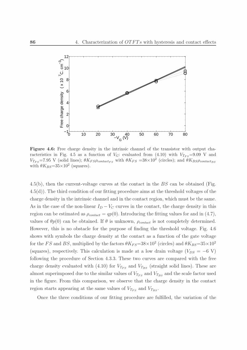
86 4. Characterization of OTFTs with hysteresis and contact effects
0 10 20 30 40 50 60 70 80−1
0
2
4
6
8
10
12
−VG
(V)
Fre
e ch
arge
den
sity
(
x 10
7C
. cm
−3 )
Figure 4.6: Free charge density in the intrinsic channel of the transistor with output cha-racteristics in Fig. 4.5 as a function of VG: evaluated from (4.10) with VTFS
=9.09 V andVTFS
=7.95 V (solid lines); θKFSρcontactFSwith θKFS =38×102 (circles); and θKBSρcontactBS
with θKBS=35×102 (squares).
4.5(b), then the current-voltage curves at the contact in the BS can be obtained (Fig.
4.5(d)). The third condition of our fitting procedure aims at the threshold voltages of the
charge density in the intrinsic channel and in the contact region, which must be the same.
As in the case of the non-linear ID − VC curves in the contact, the charge density in this
region can be estimated as ρcontact = qp(0). Introducing the fitting values for and in (4.7),
values of θp(0) can be obtained. If θ is unknown, ρcontact is not completely determined.
However, this is no obstacle for the purpose of finding the threshold voltage. Fig. 4.6
shows with symbols the charge density at the contact as a function of the gate voltage
for the FS and BS, multiplied by the factors θKFS=38×102 (circles) and θKBS=35×102
(squares), respectively. This calculation is made at a low drain voltage (VDS = −6 V)
following the procedure of Section 4.3.3. These two curves are compared with the free
charge density evaluated with (4.10) for VTFSand VTBS
(straight solid lines). These are
almost superimposed due to the similar values of VTFSand VTBS
and the scale factor used
in the figure. From this comparison, we observe that the charge density in the contact
region starts appearing at the same values of VTFSand VTBS
.
Once the three conditions of our fitting procedure are fulfilled, the variation of the

4.4. Results and Discussion 87
trapped particles per unit area can be evaluated from (4.1). However, prior to the analy-
sis of the data in Fig. 4.5, we show a case where one of the conditions of our fitting
method are not fulfilled, and how our method solves this problem. Fig. 4.7 shows output
characteristics with hysteresis measured in the same transistor as in Fig. 4.5 (symbols)
[13]. In Fig. 4.5, the gate voltage sweeps from –20 to –80 V with a −20 V step (OFF-
to-ON). In Fig. 4.7, the gate voltage sweeps from ON-to-OFF (-80 to -20 V) with a 20
V step. These current voltage curves in the FS and BS are compared with the compact
model (4.2). The parameters used in the fitting are the same as in Fig. 4.5 except the
parameter RC . The values of this parameter for forward and backward sweeps for each
VG are given in Table 4.3.
Table 4.3: Extracted values of RCFSand RC−BS for the pentacene single-crystal sample with
output characteristics in Fig. 4.7.
VG (V olts) RCFS(Ω) RCBS
(Ω)-20 7.0× 10⁶ 7.0× 10⁶
-40 2.9× 10⁶ 2.6× 10⁶
-60 1.7× 10⁶ 1.4× 10⁶
-80 1.1× 10⁶ 1.0× 10⁶
For the experimental data of Fig. 4.7(a) and (b), the evaluation of the free charge den-
sity in the device with VG in the FS and BS can be seen in Fig. 4.7(c). The charge density
at the contact during the FS and BS (ρcontactFSand ρcontactBS
, respectively), estimated
as ρcontact=qp(0), is evaluated at VDS = −6 V and following the procedure described in
Section 4.3.3. These charge densities are multiplied by the factors θKFS=11×103 and
θKBS=11×103 (circles and squares, respectively). The resulting curves are compared
with (4.10) evaluated at VTFSand VTBS
(straight solid lines). According to Fig. 4.7(c),
the charge density in the intrinsic channel and in the contact region starts appearing at
different threshold voltages: ≈+9 V and ≈-8.5 V, respectively. This result means that
the set of fitting parameters do not provide a good physical solution, despite the good
agreement between the experimental data and the results of the compact model (4.2).
Under this circumstance, the iterative procedure must be repeated using the average
values of the threshold voltages obtained for the intrinsic channel and contact regions in
FS and BS:VTFS=0 V and VTBS
=-1 V, respectively. Parameters γ and µo are maintained
equal to the previous solution, and parameters RC are searched in order to get a new

88 4. Characterization of OTFTs with hysteresis and contact effects
−80 −60 −40 −20 0−60
−40
−20
0
VD
(V)
I D (
µ A
)
−80 −60 −40 −20 0−60
−40
−20
0
VD
(V)
I D (
µ A
)
−10 0 20 40 60 800
5
10
15
20
25
30
Fre
e ch
arge
den
sity
( x
10
7 C
. cm
−3 )
−VG
(V)
(b)
(a)
(c)
Figure 4.7: (a), (b) Comparison of experimental output characteristics (FS , circles; and BS,squares) of a pentacene single crystal field effect device [13], with our compact model (solidline). VG is swept from - 80 to 0 V (ON-to-OFF) with a 20 V step. The values of the fittingparameters RCFS
and RCBSare in Table. 4.3. (c) Free charge density in the intrinsic channel as
a function of VG: evaluated from (4.10) with VTFS= 9.09 V and VTBS
= 7.95 V (superimposedsolid lines); ρcontactFS
with θKFS = 11 × 103 (circles) and ρcontactBSwith θKBS = 11 × 103
(squares).
agreement between the experimental data and our compact model. This is shown in Fig.
4.8(a) and (b). The new set of values for the parameter RC in (4.7) for forward and
backward sweeps for each VG are given in Table 4.4.
Table 4.4: Extracted values of RCFSand RC−BS for the pentacene single-crystal sample with
output characteristics in Fig. 4.7.
VG (V olts) RCFS(Ω) RCBS
(Ω)-20 5.00× 10⁶ 5.00× 10⁶
-40 2.45× 10⁶ 2.20× 10⁶
-60 1.55× 10⁶ 1.35× 10⁶
-80 1.05× 10⁶ 0.95× 10⁶

4.4. Results and Discussion 89
−80 −60 −40 −20 0−60
−40
−20
0
VD
(V)
I D (
µ A
)
−80 −60 −40 −20 0−60
−40
−20
0
VD
(V)
I D (
µ A
)
0 20 40 60 800
1
2
3
4
5
6
7
8
9
10
11
Fre
e ch
arge
den
sity
(x
10 7
C. c
m−
3 )
−VG
(V)
(c)
(b)
(a)
Figure 4.8: (a), (b) Comparison of experimental output characteristics (FS , circles; and BS,squares) of a pentacene single crystal field effect device [13], with our compact model (solidline). VG is swept from - 80 to 0 V (ON-to-OFF) with a 20 V step. The values of the fittingparameters RCFS
and RCBSare in Table. 4.4. (c) Free charge density in the intrinsic channel
as a function of VG: evaluated from (4.10) with VTFS= 0 V and VTBS
= −1 V (superimposedsolid lines); ρcontactFS
and ρcontactBSwith θKFS = 42 × 103 (circles) and θKBS = 39 × 103
(squares).
For this solution, the evaluation of the free charge density in the device with VG in
the FS and BS can be seen in Fig. 4.8(c). The charge densities at the contact during
the FS and BS ( ρcontactFSand ρcontactBS
, respectively), estimated as ρcontact=qp(0), are
evaluated at VDS = –6 V following the procedure described in Section 4.3. The charge
density at the contact is multiplied by the factors θKFS=42×102 and θKBS=39×102
(circles and squares, respectively). This solution shows how the threshold voltages of the
charge density in the contact and in the intrinsic channel coincide.
Once a physical solution has been obtained, the variation of trapped particles per
unit area can be extracted from the output characteristics of the intrinsic transistor.
The variation ∆P is obtained from (4.1) evaluated at VDS = –6 V and different gate
voltages. The equivalent drain-terminal voltage is VD = VDS+VS ≈ –10 V. Fig. 4.9 shows,

90 4. Characterization of OTFTs with hysteresis and contact effects
20 30 40 50 60 70 800
0.5
1
1.5
2
2.5
−VG
(V)
Var
iatio
n of
trap
ped
part
icle
s,
∆ P
(x
1011
cm
−2 )
(b)
(a)
Figure 4.9: Variation of the concentration of trapped particles per unit area as a function ofthe gate voltage. (a) ∆P is extracted from (4.1) at VDS =–6 V (∆(ID(VDS , VG)). (b) ∆P isextracted from (4.1) at VD = –10 V (∆(ID(VD, VG)); VDS and VD are related by the contactvoltage VS ≈ −4 V. Circles and squares represent the OFF-to-ON case of Figs. 4.5(a) and (b),and the ON-to-OFF case of Figs. 4.8(c) and (d), respectively.
in solid lines with symbols, the result of this calculation as a function of gate voltage
for the OFF-to-ON case (circles) and the ON-to-OFF case (squares). On average, the
variation of the concentration of trapped particles per unit area is ∆P = 1.24 × 10¹¹
cm−2 and ∆P = 2.1 × 1011 cm−2 for the FS and BS, respectively. These values are in
agreement with the values obtained for the same transistors by transient experiments
[13].
The advantage of our procedure is the use of a compact model that describes the
output characteristics of the transistor measured with the two-terminal method. Essential
parameters such as the threshold voltage and the mobility, the contact voltage and a
solution of the variation of trapped charge during a hysteresis cycle are determined
with these experimental and modelling tools. Other techniques, such as the transient
experiments need to be complemented with other measurements (transfer or output
curves) in order to determine all this information. The use of other models that do not
consider the contact effects properly may alter the results significantly. Fig. 4.9 shows,
in dotted line with symbols, the results of evaluating the concentration of the trapped
particles per unit area by considering the output characteristics of the transistors referred
to its terminal voltages ID(VD, VG), instead of using the intrinsic transistor response.

4.4. Results and Discussion 91
They are evaluated for VD = –10 V, which is related to VDS = –6 V by the contact
voltage (VS ≈ 4 V). We observed a decrease of one order of magnitude compared to the
results obtained by the analysis of the intrinsic transistor (i.e. by eliminating the contact
effects). This difference in the results obtained by considering the contact region or not
are treated in detail in the next chapter.

92 4. Characterization of OTFTs with hysteresis and contact effects

5
Variation of the Trapped Charge in
OTFTs during Hysteresis
5.1. Introduction . . . . . . . . . . . . . . . . . . . . . . . . . . . . 94
5.2. Variation of the trapped charge in voltage cycling . . . . . . 96
5.3. Transistor models . . . . . . . . . . . . . . . . . . . . . . . . . 97
5.4. Results and discussion . . . . . . . . . . . . . . . . . . . . . . 100
5.4.1. Transistors with linear contacts . . . . . . . . . . . . . . . . . . 100
5.4.2. Transistors with non-linear contacts . . . . . . . . . . . . . . . 107
93

94 5. Variation of the Trapped Charge in OTFTs during Hysteresis
5.1. Introduction
In Chapter 2, we proposed a method to extract the voltage drop at the contact region
from the output characteristics of the transistor [86][83]. The basis of this method is the
combination of a characterization technique [73] with a compact model that incorporates
the effect of the contacts in both the drain and gate voltages, and the mobility and the
threshold voltage [9]. In Chapter 4, we applied this method to curves with hysteresis.
Hysteresis adds the problem of working with a variable threshold voltage from the forward
sweep (FS) to the backward sweep (BS), and even during each sweep. We proposed a
solution to overcome this inconvenience during the extraction process [91].
In the literature, we can find studies that characterize the hysteresis in OTFTs from
transfer and output characteristics. In some cases, contact effects are not considered
[13]. In other cases, contact effects are eliminated from the experimental data by using
elaborate experimental procedures such as the four-terminal method, instead of the usual
two-terminal one [14]. Different results are obtained depending on the characterization
method and the importance given to the contact region of the transistor. The complete
isolation of the intrinsic transistor from the contact region should be essential to obtain
accurate results. Other studies analysing different properties of OTFTs, such as the
low-frequency noise, showed the importance of determining the correct voltage across
the intrinsic channel by removing previously the contact resistance [88].
In this chapter, we propose a precise way to remove the contact voltage from the
output characteristics of an OTFT. The objective is to determine accurately the variation
of trapped charge produced during voltage cycling in the output characteristics of the
transistor.
In the previous chapters, we have developed and checked a method to extract the
current-voltage curves at the contact (ID = ID(VS)) and the output characteristics of the
intrinsic transistor (ID = ID(VDS, VGS)) from the experimental curves (ID = ID(VD, VG))
(Fig. 5.1). Once these curves are extracted, the variation of the trapped charge during a
hysteresis cycle can be determined considering the variations of the drain current during
a hysteresis cycle. In the previous chapter, we determined the variation of the trapped
charge by analysing the variation of the curves ID(VDS , VG). In that case, we assumed
VGS ≈ VG. In this chapter, we determine this variation of the trapped charge by analysing
the intrinsic transistor, described by the ID = ID(VDS, VGS) curves (Fig. 5.1). We also

5.1. Introduction 95
Figure 5.1: The proposed equivalent circuit of a TFT including a voltage drop at the sourcecontact VC ≡ VS [83].
evaluate this variation directly from the experimental ID = ID(VD, VG) curves. All these
cases intend to reproduce characterization methods found in the literature where the
contacts are treated in different ways [13][14].
Other situations can be analysed, as the contact effects have been treated and mo-
delled extensively in the past. There are models that remove the contact effects mainly
from the drain-terminal voltage, provide excellent fittings with the experimental data,
and extract the contact I-V curves from the experimental ones [59][67][36]. It is our ob-
jective to determine the variation of the trapped charge produced during a hysteresis
cycle under the conditions imposed by all these models and to compare their results.
Even the classical MOS model is analysed, in order to quantify the effect of neglecting
the contact effects completely. The objective is to find out whether it is worth dealing
with a more elaborate and precise characterization procedure instead of working with a
simpler but less precise one; or whether it is worth extracting the intrinsic current vol-
tage curves of the OTFT instead of working directly with the experimental data. This
is discussed in this chapter.

96 5. Variation of the Trapped Charge in OTFTs during Hysteresis
5.2. Variation of the trapped charge in voltage cy-
cling
Hysteresis phenomena can appear in output (ID–VD) and in transfer (ID–VG) curves
of OTFTs. In case no contact effects are present (VC = 0 in Fig. 5.1), a way to determine
the variation of the trapped charge is by measuring the displacement current or difference
in the drain current between forward- (FS) and backward-sweep (BS) curves, at certain
values of the drain and gate voltages, ∆ID = ∆ID(VD, VG). The relation between the
variation of the trapped particles ∆P in the intrinsic channel of a transistor and the
current displacement ∆ID = ∆ID(VD, VG) is given by [13]:
∆P =∆ID × L
q × w × VD × µ(5.1)
where q is the elementary charge, µ is the charge carrier mobility, L and w are the channel
length and width of the transistor’s organic material, respectively. In case contact effects
are present, (VC 6= 0), we propose to determine the variation of the trapped particles by
measuring the difference in the drain current between the FS and BS that occurs in the
intrinsic channel of the transistor, ∆ID = ∆ID(VDS , VGS), (Fig. 5.1):
∆P =∆ID × L
q × w × VDS × µ(5.2)
The results obtained by substituting ∆ID(VDS, VGS) in (5.2) are expected to be free
of contact effects, and thus, close to the actual results.
The process of extraction of the output characteristics of the intrinsic transistor
ID(VDS, VGS) begins by extracting the curves ID = ID(VDS) and ID(VS) from the measu-
red output characteristics ID(VD) at VG = constant. The process of extraction considers
that ID = ID(VS) = ID(VDS) = ID(VD) and VD = VDS + VS at VG = constant. 5.2 shows
two examples of this procedure applied to transistors analysed in this work [87][14]. Sub-
sequently, a simple numerical treatment of the curves ID = ID(VDS) and ID(VS) at VG =
constant provides a set of curves for the intrinsic transistor: ID(VDS) at VGS = constant.

5.3. Transistor models 97
−10 −5 0
−5
−4
−3
−2
−1
0
VD
, VDS
, VC
(V)
I D (
n A
)
−40 −20 0
−200
−150
−100
−50
0
V D
, VDS
, VC
(V)
I D (
µ A
)
(b)
VG
= −32 V
(a)
VG
= −10 V
ID
(VDS
)ID
(VD
) ID
(VC
)ID
(VD
) ID
(VC
) ID
(VDS
)
Figure 5.2: Extraction of current-voltage curves of the intrinsic channel, ID(VDS), and thecontact, ID(VS), from experimental curves measured at the external terminals of OTFTs,ID(VD). ID = ID(VS) = ID(VDS) = ID(VD) and VD = VDS + VS. The transistors show (a)linear [87] and (b) non-linear ID(VS) curves at the contacts [14]. In a second step, curvesID(VDS) at VGS = constant can be obtained. The dashed and solid lines represent the forward(FS) and backward sweeps (BS), respectively.
5.3. Transistor models
The process of separating the contact and intrinsic contributions in the OTFT, requi-
res a model that incorporates the contact effects. As the basis of this work, we consider
the compact model that presented in Chapter 2. It describes the output characteristics
in a transistor as [83][73]:
IDL
w=
µoCi
γ + 2[(VG − VT − VS)
γ+2 − (VG − VT − VD)γ+2] (5.3)
ID =VS
RC
, or ID = MV 2S
where Ci is the gate insulator capacitance per unit area, VT is the threshold voltage, µo is
the mobility at zero electric field (µ = µo(VG − VT ) ) and µ is the mobility enhancement
factor. The contact voltage VS is modelled by a linear or non-linear relation with ID

98 5. Variation of the Trapped Charge in OTFTs during Hysteresis
depending on the behaviour of the output characteristics at low drain voltage. The
advantages of this method is that it clearly distinguishes the contact voltage VS from the
terminal voltages VG and VD.
There are models that eliminate the contact voltage only from the drain-terminal
voltage [59][67][36]. They can be used instead of our compact model to obtain the intrinsic
and contact contributions. However, they represent an intermediate situation between a
compact model that eliminates the effect of the contacts from both the drain and gate
terminals, and the classical MOS model that neglects all these effects:
ID =wµoCi
L[(VG − VT )VD − V 2
D
2], VD < VG − VT (5.4)
ID =wµoCi
2L[(VG − VT )
2], VD ≥ VG − VT
In order to consider the effect of analysing an OTFT under a generic intermediate
situation, we consider a modification of (7.1), while maintaining the model of the contact
region of (5.3). It assumes that the contacts affect only on the drain voltage (VDS =
VD–VS) while VGS ≈ VG. Thus, this modification affects only the triode region in (7.1):
ID =wµoCi
L[(VG − VT )VDS − V 2
DS
2] (5.5)
ID =wµoCi
2L[(VG − VT )
2], VD ≥ VG − VT
ID =VS
RC
, or ID = MV 2S
In the following section, we determine the variation of the trapped particles (∆P )
from output characteristics with hysteresis taken from the literature [14][87], using the
models (5.3)-(5.5) (Table 5.1). The objective is to determine which parameter or variable
is affected the most by the contact region: the mobility or the gate- and drain-terminal
voltages.
In procedures # 1, # 2 and # 3 of Table 5.1, the transistor is modelled with the
compact model (5.3). ∆P is extracted from variations in the drain current referred to:
the intrinsic voltages (VDS and VGS) (procedure # 1); the intrinsic VDS and the external
VG (procedure # 2); and the external VG and VD (procedure # 3). The mobility in these

5.3. Transistor models 99
three cases is assumed free of contact effects and the same in all of them, as the compact
model is used to reproduce the experimental output characteristics.
To analyse the effect of the mobility on the determination of ∆P , model (5.5) is also
used to fit the experimental data (procedures # 4 and # 5). Basically, the mobility and
the threshold voltage are extracted from the saturation region. Therefore, no relation
to the contact region is established. The contact parameters, RC or M , are extracted
from the triode region. In procedure # 4, the variation of the drain current is referred to
the intrinsic VDS and the external VG. In procedure # 5, ∆P is referred to the external
voltages VD and VG. This last case represents the worst scenario as contact effects are
neglected in both the mobility and terminal voltages. Procedures # 2, # 3 and # 4
represent intermediate situations between the best and worst scenarios. In any case, we
aim to find out how far these situations are among each other, and whether a good
approximation to case # 1 exists or not, in order to obtain more simple calculations.
These procedures are applied to the linear regime of the transistor, where the variation
of the trapped charge is evaluated at different gate and drain voltages. The output
characteristics affected by contact effects show typically two different trends at low drain
voltages. Non-linear [75][60][59], and linear relations [75][22][92] can be observed in this
low drain voltage region. In this work, we analyze output characteristics taken by different
authors showing both trends (Fig. 5.2) [14][87].
Table 5.1: Procedures to determine the variation of the trapped particles (∆P ) during ahysteresis cycle in the transistor. The ∆P is extracted analysing the variations of the draincurrent referred to the voltages at the external terminals (5.1) or at the intrinsic transistor(5.2). The intrinsic voltages are extracted employing the compact model (5.3) or model (5.5).The effect of the contact voltage on the mobility is also checked. Two different values for themobility are extracted: one extracted from the compact model (5.3) and another from model(5.5).
Procedure ∆P I − V Correction of contact Mobility Correction of contactModel Model effects on terminals model effects on µ
# 1 (5.2) (5.3) VD, VG (5.3) Y es# 2 (5.2) (5.3) VD (5.3) Y es# 3 (5.1) (5.3) none (5.3) Y es# 4 (5.2) (5.5) VD (5.5) No# 5 (5.1) (5.5) none (5.5) No

100 5. Variation of the Trapped Charge in OTFTs during Hysteresis
5.4. Results and discussion
5.4.1. Transistors with linear contacts
Figs. 5.3(a) and (b) show with symbols output characteristics with hysteresis measu-
red in a pentacene single crystal TFT [87]. In this transistor, the gate dielectric thickness
is ti = 1µm , the channel length L=100 µm, the transistor width w = 1 mm, the organic-
film thickness to = 100 nm. The drain-source electrodes are deposited through a shadow
mask and the metal thicknesses are Cr = 5 nm and Au = 40 nm. These current voltage
curves in the FS and BS are compared with the compact model (5.3) in combination
with the linear model (5.6) for the current-voltage curves at the contact, as the output
characteristics show a linear trend at low VD values. Our numerical results are shown in
solid lines in Fig. 5.3(a) and (b). The parameters obtained from the fitting procedure
are: µo = 0.0041 cm2/(Vs), γ = 0.05, VTFS= 5.18 V and VTBS
= 3.55 V. Parameter RC
in (5.6) for forward and backward sweeps for each VG is given in Table. 5.2.
ID ≈ qSp(0)µθVC/xC ≡ VC/RC (5.6)
Table 5.2: Extracted values from model (5.3) of RCFSand RC−BS for the pentacene single-
crystal sample with output characteristics in Fig. 5.3.
VG (Volts) RCFS(Ω) RCBS
(Ω)0 14× 109 10× 109
-2 10× 109 6.0× 10⁹
-4 6.0× 10⁹ 3.8× 10⁹
-6 3.0× 10⁹ 2.1× 10⁹
-8 1.8× 10⁹ 1.3× 10⁹
-10 1.2× 10⁹ 1.0× 10⁹
Combining in (5.3) the above values of µo, γ and VTFSwith the experimental values
(ID, VD) of Fig. 5.3(a), then the current-voltage curves at the contact in the FS can
be obtained. The result is seen in Fig. 5.3(c), where an almost perfect linear trend
is observed, as expected. Repeating the same procedure with the experimental values
(ID, VD) of Fig. 5.3(b), then the current-voltage curves at the contact in the BS can be
obtained (Fig. 5.3(d)). The third condition of our fitting procedure aims at the threshold

5.4. Results and discussion 101
voltages of the charge density in the intrinsic channel and in the contact region, which
must be the same. The charge density in this region can be estimated as ρcontact = qp(0).
Introducing the fitting values for RCFSand RCBS
in (5.6), values of θp(0) can be obtained.
If θ is unknown, ρcontact is not completely determined. However, this is no obstacle for
the purpose of finding the threshold voltage. Fig. 5.4 shows with symbols the charge
density at the contact as a function of the gate voltage for the FS and BS, multiplied
by the factors θKFS = 1 × 10⁴ (circles) and θKBS = 5 × 10⁴ (squares), respectively.
This calculation is made at a low drain voltage (VDS = -2 V) following the procedure of
Section 4.3.3. These two curves are compared with the free charge density evaluated as
ρchannel = Ci(VGS − VT )/to (5.7)
for VTFSand VTBS
. From the comparison in Fig. 5.4, we observe that the charge density
in the contact region starts appearing at the same values of VTFSand VTBS
.
Once the results of these tests have physical meaning, the current voltage curves of the
intrinsic transistor and of the contact region can be extracted following the procedures
described in Sec. 5.3. From these curves, the variation of the trapped charge can be
determined. Fig. 5.5 illustrates some steps of these extraction procedures.
Procedure #1. Fig. 5.5(a) shows the drain current as a function of the gate
voltage VGS at VDS = 2 V. The variation of the drain current from Fig. 5.5(a) can
be introduced in (5.2) to determine ∆P as a function of VGS . The average value
over VGS is ∆P = 2 × 1010 cm−2. This procedure is repeated at different values
of VDS in the linear region. The result is represented with circles in Fig. 5.6. The
average value over VDS and VGS in this region is ∆P (#1) = 2.47× 1010 cm−2. By
referring ∆P to the intrinsic voltages VDS and VGS, we eliminate any relation to the
contact region. The mobility is also free from contact effects as the experimental
data have been reproduced by (5.3). To analyse the difference of working with the
intrinsic voltages or with terminal voltages, we study the following two procedures.
Procedure #2. This case considers the effect of the contact region on the gate
terminal. The variation of the trapped charge is analysed as a function of VDS
and VG. Solid lines in Fig. 5.5(b), show the drain current as a function of VG at
VDS = 2 V. By introducing the variation of the drain current ∆ID(VDS, VG) in

102 5. Variation of the Trapped Charge in OTFTs during Hysteresis
−10 −5 0−5
−4
−3
−2
−1
0
VD
(V)
I D (
nA)
−10 −5 0−5
−4
−3
−2
−1
0
VD
(V)
I D (
nA)
−5 −4 −3 −2 −1 0−5
−4
−3
−2
−1
0
VC
(V)
I D (
nA)
−6 −5 −4 −3 −2 −1 0−5
−4
−3
−2
−1
0
VC
(V)
I D (
nA)
(a)
(b)
(c)
(d)
Figure 5.3: (a), (b) Comparison of experimental output characteristics of a top gate coplanarPVA / pentacene / Au OFET [87], with our compact model (solid line); (c), (d) Extractedcurrent voltage curves at the contact region. VG = 0 to −10 V from top to bottom with a −2V step (FS, circles; and BS, squares).
(5.2), the variation ∆P can be obtained. The average value over VG evaluated at
VDS = –2 V is ∆P = 0.6× 1010 cm−2, lower than in procedure #1. Repeating this
calculation at different values of VDS in the linear region, we obtain the squares in
Fig. 5.6. The average value over VDS and VG is ∆P (#2) = 0.3 × 1010 cm−2. The
relative difference between procedure #1 and #2 is 88%.
Procedure #3. In this case, the variation of the trapped charge is extracted
directly from the experimental data ID = ID(VD, VG). We analyse the effect of
working with the terminal voltages instead of the intrinsic ones. However, the
mobility is extracted from the fitting of the experimental data with (5.3). This
situation might be interesting if these results were close to the ones in procedure
#1, since no computational time is needed to determine ID as a function of the
intrinsic voltages. The dotted lines in Fig. 5.5(b) show the drain current as a

5.4. Results and discussion 103
0 2 4 6 8 100
5
10
15
20
25
−VG
(V)
Fre
e ch
arge
den
sity
(x
10 8 C
. cm
−3 )
Figure 5.4: Free charge density in the intrinsic channel of the transistor with output cha-racteristics in Fig. 5.3 as a function of VG: evaluated from (4.10) with VTFS
= 5.18 V andVTBS
= 3.55 V (solid lines); θKFSρcontactFSwith θKFS = 1× 10⁴ (circles); and θKBSρcontactBS
with θKFS = 5× 10³ (squares).
function of VG at VD = −2 V. By introducing the variation of the drain current
∆ID(VD, VG) in (5.1), ∆P can be obtained. The average value over VG evaluated at
VD = −2 V is ∆P = 0.93×1010 cm−2, lower than in procedure #1. Repeating this
calculation at different VDS , we obtain the crosses in Fig. 5.6. The average value of
∆P over VD and VG is ∆P (#3) = 0.77× 1010 cm−2. The relative different between
procedure #1 and #3 is 68%. This relative variation is better than in procedure
#2, however this result disregards the possibility of using directly the experimental
data to obtain an accurate value of ∆P . Otherwise, we have to be conscious of the
error we manage with.
Procedure #4. In procedures #4 and #5, we consider the effect of the contacts
on the mobility and how this variable affects the determination of ∆P . We consider
model (5.5) with ID = VC/RC to fit the same experimental data of Fig. 5.3. The
fitting of the experimental data with model (5.5) can be seen in Figs. 5.7(a) and
(b). In this case, another set of fitting parameters is obtained: µo = 0.0024 cm2/
Vs and VT = 0.6 V for both FS and BS. The parameter RC in (5.5) for forward

104 5. Variation of the Trapped Charge in OTFTs during Hysteresis
0 5 100
0.5
1
1.5
2
−VG
(V)
−I D
(n
A)
0 5 100
0.5
1
1.5
2
2.5
3
3.5
−VGS
(V)
−I D
(n
A)
(b)(a)
VDS
constant
= −2V
VD
constant
= −2V
Figure 5.5: Transfer characteristics corresponding to the transistor in Fig. 5.3 [87]. (a) Proce-dure #1, intrinsic transistor, ID(VGS) at VDS = −2 V. (b) Procedure # 3, external terminals,ID(VG) at VD = −2 V (dotted lines); and procedure # 2, intermediate situation, ID(VG) atVDS = −2 V(solid lines). (FS, circles; and BS, squares).
−4 −3.5 −3 −2.5 −20
5
10
15
20
25
30
VD
, VDS
(V)
Var
iatio
n of
trap
ped
part
icle
s (x
10 9 c
m−
2 )
Variation referred to:
VDS
,VGS
VD
,VG
VDS
,VG
Figure 5.6: Variation of trapped particles obtained from the hysteresis cycles in Fig. 5.3.Intrinsic transistor, #1, (circles); intermediate situation, #2, (squares); external terminals,#3, (crosses).

5.4. Results and discussion 105
−10 −5 0−5
−4
−3
−2
−1
0
VD
(V)
I D (
nA)
−10 −5 0−5
−4
−3
−2
−1
0
VD
(V)
I D (
nA)
BS
FS
Figure 5.7: Comparison of the same experimental output characteristics of Fig. 5.3 (circlesFS; and squares BS) with model (5.5) (solid lines). VG = (-2, -4, -6, -8, -10) V from top tobottom
and backward sweeps for each VG is given in Table 5.3. Although a good fitting
is obtained, it does not mean that the fitting parameters have a good physical
meaning, as has been checked positively with the ones extracted from model (5.3).
An extensive discussion on how to select a proper value for the threshold voltage
from curves with hysteresis was done in Chapter 4 [91].
Table 5.3: Extracted values from model 5.5 of RCFSand RCBS
for the pentacene single-crystalsample with output characteristics in Fig. 5.7.
VG (V olts) RCFS(Ω) RCBS
(Ω)0 55× 108 20× 108
-2 40× 108 18× 108
-4 35× 108 15× 108
-6 17× 108 8.0× 10⁸
-8 8.0× 10⁸ 4.0× 10⁸
-10 3.5× 10⁸ 2.5× 10⁸
Once this agreement is achieved, the curves ID(VDS) for VG = constant can be

106 5. Variation of the Trapped Charge in OTFTs during Hysteresis
0 2 4 6 8 100
0.5
1
1.5
−VG
(V)
−I D
(n
A)
Figure 5.8: Transfer characteristics, ID(VG) at VDS = −2 V, after the fitting of the experi-mental data [87] in Figs. 5.7(a) and (b) with model (5.5). (FS, circles, and BS, squares).
extracted from the experimental data, as detailed in Sec. 5.3. One of the results
the extraction process is shown in Fig. 5.8, where ID is represented as a function
of VG at VDS = −2 V. The variation of the drain current from Fig. 5.8, ∆ID =
∆ID(VDS , VG), can be inserted in (5.2) to determine ∆P as a function of VG. At
VDS = −2 V, the average value over VG is ∆P = 0.09× 1010 cm−2. This procedure
is repeated at different values of VDS in the linear region. The average value over
VDS and VG in this region is ∆P (#4) = 0.74× 1010 cm−2. In order to analyze the
effect of the contact region on the mobility, we can compare this result with the
one in procedure #2, as ∆ID is referred to the voltages VDS and VG, in both cases.
Despite using different models, the ratio of ∆P between procedures #2 and #4 is
similar to the ratio of the values of the mobility obtained with the models (5.3)
and (5.5): µ (model (5.3)) /µ (model (5.5)) (=ratio of the values of the mobility
extracted from the models (5.3) and (5.5)).
Procedure #5. In this procedure, we consider the external voltages of the tran-
sistor (VD, VG), not the intrinsic ones. The variation of the trapped particles is
determined by introducing ∆ID = ∆ID(VD, VG) in (5.1). At VD = −2 V, the ave-
rage value of ∆P over VG is ∆P = 0.16 × 1010 cm−2. This calculation is repeated

5.4. Results and discussion 107
at different values of VD in the linear region. The averaged result over VD and VG
in this region is ∆P = 1.44×1010 cm−2. This result can be compared with the one
in procedure #3. Both procedures use (5.1) to determine ∆P . Thus, (∆P (#5)) /
(∆P (#3)) ≈ µ (model (5.3)) /µ (model (5.5)).
By comparing the result of procedure #1 with the rest, we observe that neglecting
the effect of the contact region on the terminal voltages reduces the value of ∆P .
∆P is also reduced when the contact region is not considered in the determination
of the mobility. Both reductions are similar. In the case studied above, the factor γ,
that represents the dependence of the mobility on the gate voltage, is close to zero.
A greater value of γ would enhance the difference of results among the procedures.
The relative variation of ∆P among the different procedures ranges from 70% to
98% . A summary of these results is seen in Table 5.4.
Table 5.4: Average variation of the trapped charge ( P ) in the linear region during ahysteresis cycle in two kinds of OTFT ( showing linear and non-linear contact current-voltagecurves).
Linear ID − VC curves Non-Linear ID − VC curvesProcedure ∆P (cm−2) µ (cm2/Vs) ∆P (cm−2) µ (cm2/Vs)
#1 2.47 ×10¹⁰ 0.0041 2.21 ×10¹¹ 0.38#2 0.30 ×10¹⁰ 0.0041 0.32 ×10¹¹ 0.38#3 0.77 ×10¹⁰ 0.0041 1.52 ×10¹¹ 0.38#4 0.06 ×10¹⁰ 0.0245 0.27 ×10¹¹ 1.80#5 0.13 ×10¹⁰ 0.0245 0.32 ×10¹¹ 1.80
5.4.2. Transistors with non-linear contacts
In this section, we repeat the previous analysis on OTFTs showing a non-linear
response at low values of the drain voltage. The objective is to analyse whether different
behaviours of the current voltage curves at low values of the drain voltage affect the
results. Fig. 5.9 shows output characteristics with hysteresis measured in a rubrene single
crystal TFT [14] (symbols).
In this transistor, the gate dielectric thickness is ti = 0.3µ m, the channel length
L=16 µ m, the transistor width w=500 µ m and the organic-film thickness to=5 µ m.

108 5. Variation of the Trapped Charge in OTFTs during Hysteresis
−40 −30 −20 −10 0−200
−150
−100
−50
0
VD
(V)
I D (
µ A
)
−40 −30 −20 −10 0−200
−150
−100
−50
0
VD
(V)
I D (
µ A
)
−40 −30 −20 −10 0−200
−150
−100
−50
0
VD
(V)
I D (
µ A
)
−40 −30 −20 −10 0−200
−150
−100
−50
0
VD
(V)
I D (
µ A
)
(a)
(b)
(c)
(d)
Figure 5.9: Comparison of the experimental (circles FS; and squares BS ) output characte-ristics of a rubrene transistor in [14] , (a) and (b) with model (5.5) (solid lines), (c) and (d)with model (5.3) (solid lines). VG = (-8, -12, -16, -20, -24, -28, -32) V from top to bottom.
The experimental I − V curves in the FS and BS are compared with the compact
model (5.3) (solid lines in 5.9(c) and (d)) and with the model (5.5) (solid lines in Fig.
5.9(a) and (b). The output characteristics show a non-linear trend at low VD. In this
case, ID = MV 2C is employed in (5.3) and (5.5) to model the contact region. The fitting
parameters from model (5.3) are extracted following the procedure developed in Chapter
4 [91]: µo = 0.38 cm2 / (Vs), γ = 0 , VTFS=- 0.36 V and VTBS
= -0.4 V for the FS and
BS. The parameter M in (5.3) for forward and backward sweeps for each VG is given in
Table 5.5.
In the case of model (5.5) the fitting parameters are: µo = 1.8 cm2/Vs, VT = −1 V
for both FS and BS. The parameter M in (5.5) for forward and backward sweeps for
each VG is given in Table 5.5.
Once the experimental data have been reproduced with models (5.3) and (5.5) and
all fitting parameters are known, the current voltage curves of the intrinsic transistor and
of the contact region can be extracted in both situations, and from them, the variation

5.4. Results and discussion 109
of the trapped charge. Procedures #1, #2 and #3 analyse the curves extracted with
model (5.3) and procedures #4 and #5 the curves extracted with model (5.5).
Procedure #1. Fig. 5.10(a) shows the drain current as a function of the gate
voltage VGS at VDS = −6 V. The variation of the drain current from Fig. 5.10(a)
can be introduced in (5.2) to determine ∆P as a function of VGS . The average
value over VGS is 2.34×1011 cm−2. This procedure is repeated at different values of
VDS in the linear region. The result is represented with circles in Fig.5.11(a). The
average value over VGS and VDS is ∆P (#1) = 2.21×1011 cm−2. As in the previous
case (section. 5.4.1), this procedure represents a situation where the ∆P is free
from contact effects. The effect of the contact region on the terminal voltages and
in the mobility is treated in the following procedures.
Procedure #2. This case considers the effect of the contact region on the gate
terminal. The variation of the trapped particles is analysed as a function of VDS
and VG. Solid lines in Fig. 5.10(b), show the drain current as a function of VG at
VDS = −6 V. By introducing the variation of the drain current ∆ID(VDS, VG) in
(5.2), the variation ∆P can be obtained. Its average value, evaluated over VG at
VDS = −6 V, is ∆P = 0.45 × 1011 cm−2, lower than in procedure #1. Repeating
this calculation at different values of VDS , we obtain the squares in Fig. 5.11.
The average value over VDS and VG is ∆P (#2) = 0.32 × 1011 cm−2. The relative
difference between the procedures #1 and #2 is 85%.
Procedure #3. In this case, the variation of the trapped charge is extracted
Table 5.5: Extracted values of MFS and MBS for the rubrene single-crystal sample withoutput characteristics in Fig. 4.4.
Model (5.3) Model (5.5)VG (Volts) MFS (A/V2) MBS (A/V2) MFS (A/V2) MBS (A/V2)
-8 0.90× 10⁻⁶ 0.90× 10⁻⁶ 0.50× 10⁻⁶ 1.00× 10⁻⁶
-12 1.00× 10⁻⁶ 1.00× 10⁻⁶ 1.50× 10⁻⁶ 2.00× 10⁻⁶
-16 1.10× 10⁻⁶ 1.15× 10⁻⁶ 3.60× 10⁻⁶ 3.50× 10⁻⁶
-20 1.41× 10⁻⁶ 1.46× 10⁻⁶ 3.90× 10⁻⁶ 4.30× 10⁻⁶
-24 1.42× 10⁻⁶ 1.47× 10⁻⁶ 4.00× 10⁻⁶ 4.50× 10⁻⁶
-28 1.43× 10⁻⁶ 1.48× 10⁻⁶ 4.03× 10⁻⁶ 4.60× 10⁻⁶
-32 1.44× 10⁻⁶ 1.49× 10⁻⁶ 4.08× 10⁻⁶ 4.70× 10⁻⁶

110 5. Variation of the Trapped Charge in OTFTs during Hysteresis
0 20 400
20
40
60
70
−VG
(V)
−I D
(µ
A)
0 20 400
20
40
60
80
100
−VGS
(V)
−I D
(µ
A)
VDS
con
= −6
VD
con
= −6
(a) (b)
Figure 5.10: Transfer characteristics corresponding to the transistor in Fig. 5.9 [14]. (a)Procedure #1, intrinsic transistor, ID(VGS) at VDS = −6 V. (b) Procedure # 3, externalterminals, ID(VG) at VD = −6 V (dotted lines); and Procedure # 2, intermediate situation,ID(VG) at VDS = −6 V(solid lines). (FS, circles; and BS, squares).
−10 −9 −8 −7 −6 −5 −40
50
100
150
200
250
VD
, VDS
(V)
Var
iatio
n of
trap
ped
Par
ticle
s (x
10 9 c
m−
2 )
VDS
, VGS
Variation referred to:
VDS
, VG
VD
, VG
Figure 5.11: Variation of trapped particles obtained from the hysteresis cycles as a functionof: VDS and averaged over VGS (circles); VDS and averaged VG (squares); and VD and averagedover VG (crosses).

5.4. Results and discussion 111
directly from the experimental data ID = ID(VD, VG). We work with the terminal
voltages instead of the intrinsic ones. However, the mobility is extracted from the
fitting of the experimental data with (5.3). The dotted lines in Fig. 5.10(b) show the
drain current as a function of VG at VD = −6 V. By introducing the variation of the
drain current ID(VD, VG) in (5.1), ∆P can be obtained. Its average value, evaluated
over VG at VD = −6 V, is ∆P = 1.7 × 1011 cm−2. Repeating this calculation at
different VDS, we obtain the crosses in Fig. 5.11. The average value over VDS and
VGS is ∆P (#3) = 1.5 × 1011 cm−2, lower than in procedure #1. The relative
difference between procedure #1 and #3 is 31%. This relative variation is better
than with procedure #2, but the result is not close enough to procedure #1.
In order to eliminate in situ the contact effects from the measurements, the four-
terminal method is used. Authors in [14] determine the variation of trapped charge
with this method obtaining a value of 1011 cm−2. This value lies between our results
in procedures #2 and #3, and the relative difference with procedure #1 is 60%.
Although all these results are of the same order of magnitude, it is interesting
to discuss where these differences may come from. In the four-terminal method,
the potential drop along the intrinsic channel is measured between the voltage-
probing electrodes (VC1 − VC2). They are separated such a distance from the drain
and source terminals to eliminate the voltage the potential drop at the contact
regions. The voltage drop in the intrinsic gate is estimated as the voltage VGS
between the gate contact and the channel region between these two voltage probes,
where the channel conductivity is measured: VGS = VG − (VC1 + VC2)/2. These
assumptions are necessary in order to determine the channel conductivity and the
carrier mobility [14]. However, this represents a situation where the contact effects
are eliminated from the drain to source voltage but not necessarily from the gate
voltage, corresponding to the intermediate cases considered in our work. Actually,
these authors confirmed some anomalies in the values of the mobility determined
with this method.
Procedure #4. We consider model (5.5) to fit the experimental data of Figs.
5.9(a) and (b). The values of the set of parameters (µo, γ , VT and M) extracted
with this model are different to those extracted with the model (5.3). In particular,
we can study the effect of the contacts on the mobility and how this variable affects

112 5. Variation of the Trapped Charge in OTFTs during Hysteresis
5 10 15 20 25 30 350
20
40
60
−VG
(V)
−I D
(µ
A)
Figure 5.12: Transfer characteristics of the intrinsic transistor (circles FS and square BS );extracted after the fitting of the experimental data of Fig. 5.11 with model (5.5). VDS = −6 V.
the determination of ∆P .
Once the parameter M that model the contact region, is extracted, the curve
ID = ID(VC) can be determined and the relation ID = ID(VDS, VG) can be obtained
in both FS and BS (Sec. 5.3). Fig. 5.12 shows one of the results of this calculation,
where ID is represented as a function of VG for VDS = −6 V. The variation of the
drain current ∆ID(VDS , VG) of Fig. 5.12 can be inserted in (5.2) to determine ∆P
as a function of VG. The average value evaluated over VG is ∆P = 0.26 × 10¹¹
cm−2. This procedure is repeated at different values of VDS in the linear region.
The average value over the linear region is ∆P (#4) = 0.27 × 1011 cm−2. This
result is similar to the one in procedure #2. The mobility in this procedure is
larger than the mobility in the procedure #2. However, the current voltage curves
of the contact are also different. Therefore, the effect of using different values of
the mobility is compensated with the effect of using different ID − VC curves (or a
different M parameter). We have to notice that procedures #2 and #4 represent
cases where the contact effects are not eliminated from the gate-terminal voltage.
Procedure #5. This procedure considers the curves ID−VD measured at the tran-
sistor terminals. The variation of the trapped particles is determined by introducing

5.4. Results and discussion 113
the variation of ID in (5.1). In this case, the mobility used in (5.1) corresponds to
the one extracted from model (5.5) (µo = 1.8 cm2/ Vs). Basically, the model (5.5)
without considering the contact region reduces to the classical MOS model (7.1).
At VD = −6 V, the average value of ∆P over VG is ∆P = 0.36 × 1011 cm−2. Re-
peating this calculation at different VD and averaging over VD and VG in the linear
region, the result is ∆P (#5) = 0.32×1011 cm−2. This value can be compared with
the one in procedure #3: (∆P (#3)) / (∆P (#5)) ≈ µ (model (5.5)) /µ (model
(5.3)). In these two cases, the value of the mobility is the only difference in the
evaluation of ∆P
A summary of the study of the two kinds of OTFT can be seen in Table 5.4. We can
observe how the variation of ∆P deteriorates when a non proper value of the mobility is
considered or the contact voltage is not eliminated from the terminal voltages. A proper
estimation of the mobility is essential. In that sense, a model for the OTFT including the
contact region should be used. It should determine the value of the mobility and separate
the contact voltage from the terminal voltages. The variation of the trapped charge
during a hysteresis cycle must use the current curves of the intrinsic transistor. If the
experimental data are used instead, an error of one order of magnitude can be obtained.
The worst solution is, without any doubt, when the contact voltage is eliminated partially
from the terminal voltages. The cases where the contact voltage, VC , is eliminated from
VD but not from the VG are clearly the worst of all, even considering a proper value of
the mobility.

114 5. Variation of the Trapped Charge in OTFTs during Hysteresis

6
Conclusions
115

116 6. Conclusions
1. We have made use of a physical model to interpret contact effects in orga-
nic/polymeric thin film transistors, and we have incorporated it in a generic com-
pact model that describes the output characteristics of OTFTs. The resulting
model reproduces experimental data of output characteristics showing linear and
highly non-linear responses at low drain voltages. Our model is compared with
previous circuit models proposed to explain these behaviours. Our model provides
a way to gain physical insight about the charge density in the low conductivity
region near at the contact region and mirrors the changes of charge density in the
rest of the device. Actually, the evolution with the gate voltage of the free to total
charge density ratio in the low conductivity region at the contact is in agreement
with the estimated charge density in the channel.
2. In parallel to this model, a parameter extraction procedure has been proposed in
order to determine the model parameters, including the additional ones associated
to the contact effects. The advantages of previous procedures (although less pre-
cise) are combined in our method. Although more physically advanced models are
necessary in order to take into account all the effects that appear in the OTFT ,
previous simple models cannot be completely disregarded. We have demonstrated
their usefulness in the characterization process.
3. The different steps of our procedure are monitored with experimental measure-
ments from organic thin film transistors based on Zinc Phthalocyanine and data
from other authors’ experiments.
4. In addition, we have tested the characterization method in a transistor with known
parameters obtaining no significant errors between the real parameters and the ones
extracted with the method.
5. The characterization method has also been applied to transistors which output
characteristics show both hysteresis and contact effects, making the characteriza-
tion of these transistors more difficult. We have presented a technique, based on
the previously developed compact model, to extract essential parameters, such as
the carrier mobility, the threshold voltage and the variation of the trapped charge
during a hysteresis cycle. The proposed technique overcomes the problems of ha-
ving a greater number of parameters in the model and having an internal relation
117
between some of these parameters, such as the dependence of the threshold voltage
with the trapped charge, especially at high gate voltages. The extraction of current
voltage curves of both the contact region and the intrinsic channel from the experi-
mental output characteristics has allowed for solving these problems. In particular,
the study of the evolution of the charge density with the gate voltage, in the con-
tact region and in the intrinsic channel, is essential to extract the parameters of
the transistor. Transistors showing linear and non-linear contact effects have been
studied. The results obtained with our technique have been compared with other
results provided by different authors who employed more elaborate experimental
techniques, and good agreements were obtained.
6. Different procedures to determine the variation of the trapped charge in an OTFT
during a hysteresis cycle have been presented. The procedures differ in the way
the contact effects, present in the experimental data, are treated. The procedures
separate the contribution of the intrinsic transistor and the contact region from
the experimental data. The current voltage curves of the intrinsic transistor, of
the external transistor, and of intermediate situations are used to determine the
variation of the trapped charge. A comparison of these results is provided.
7. A study of the effects of the contact region on the value of the mobility extracted
from different models has been made. A proper extraction of the mobility with
a model that incorporates contact effects is essential to obtain good results, even
if the terminal voltages are considered instead the intrinsic ones. In this regard,
a compact model that describes the output characteristics of the transistor and
includes the effect of the contact regions is considered as the best scenario. The
worst scenario is when the contact voltage is eliminated partially from the terminal
voltages.
8. The interpretation of output characteristics with hysteresis with different models
shows how the values of the variation of the trapped charge are clearly altered
by the inclusion or not of the contact effects on the terminal voltages and the
mobility. The values obtained are always different and lower than the ones obtained
with a compact model developed previously. From these results, we highlight the
importance of using a compact model that properly considers the contact effects

118 6. Conclusions
of the transistor and accurately extracts information of the trapped charge in the
semiconductor during a hysteresis cycle.

7
Resumen en espanol/Spanish
summary
7.1. Resumen . . . . . . . . . . . . . . . . . . . . . . . . . . . . . . . 120
7.2. Estructura de la Tesis . . . . . . . . . . . . . . . . . . . . . . . 122
7.3. Objetivos . . . . . . . . . . . . . . . . . . . . . . . . . . . . . . 126
7.4. Metodologıa . . . . . . . . . . . . . . . . . . . . . . . . . . . . . 126
7.5. Conceptos generales usados en la tesis . . . . . . . . . . . . . 127
7.6. Conclusiones . . . . . . . . . . . . . . . . . . . . . . . . . . . . 137
119

120 7. Resumen en espanol/Spanish summary
7.1. Resumen
El funcionamiento de los dispositivos semiconductores organicos modernos esta limi-
tado por efectos no ideales que no se caracterizan por modelos tradicionales de transporte.
En este trabajo, se estudian dos grandes problemas que afectan al comportamiento de
los transistores organicos y polimericos de lamina delgada: los efectos de los contactos y
los mecanismos de atrapamiento y emision de carga que se producen en el interior del
dispositivo. El hecho de que estos dos mecanismos esten presentes simultaneamente hace
mas complejo el estudio de estos transistores.
Se presenta en esta tesis un nuevo modelo compacto para transistores organicos de
lamina delgada (OTFT). Permite describir caracterısticas de salida de los transistores,
incorporando los efectos de los contactos. El modelo se basa en expresiones fısicamente
realistas que describen el flujo de carga en la vecindad de los contactos que se han in-
corporado en un modelo de deriva desarrollado previamente. El modelo resultante sigue
siendo compacto, al igual que el original, por lo que resulta de gran interes en simula-
ciones de circuitos con estos transistores. Un modelado adecuado necesita de parametros
que sean facilmente extraıbles a partir de medidas experimentales y que contengan una
relacion con la fısica del dispositivo. Se propone tambien un metodo para extraer los
parametros del transistor, incluyendo los nuevos parametros asociados a los contactos.
Se ha comprobado el modelo con medidas experimentales tomadas en transistores
de lamina delgada donde el material organico es ftalocianina de zinc. Los contactos de
drenador y fuente son de oro. Se analizan las respuestas de estos y otros transistores en la
zona lineal y en la de saturacion. En la region de bajas tensiones de drenador se pueden
observar en general respuestas tanto lineales como no lineales. Ambas situaciones son
analizadas en este trabajo. El metodo de extraccion de parametros sugerido en esta tesis
proporciona una forma de estudiar la evolucion de la densidad de carga en la region de
baja conductividad proxima al contacto.
El metodo de extraccion de parametros se comprueba tambien con datos obtenidos
de un transistor cuyos parametros son conocidos. Este transistor conocido es realmente
un artificio teorico que consta de un transistor ideal al que se le ha anadido en serie un
elemento de dos terminales que simula unos contactos.
Otro problema que deteriora el funcionamiento de los transistores de lamina delgada
es el mecanismo de atrapamiento y emision de carga por parte de trampas situadas en la

7.1. Resumen 121
estructura. Ello produce inestabilidades que son el origen de la histeresis en las curvas de
salida o de transferencia de los transistores. La combinacion de los fenomenos asociados
a los contactos y a la histeresis hacen que el analisis de las curvas corriente tension de
los transistores sea mas complicado. A pesar de ello se presenta un metodo de extraccion
de parametros del transistor bajo la accion de estos dos mecanismos. El metodo se basa
en el procedimiento desarrollado anteriormente en el caso de que no exista histeresis en
las muestras. La nueva tecnica de caracterizacion proporciona valores para la movilidad,
la tension umbral y la variacion de la concentracion de carga atrapada durante los ciclos
de tension. El hecho de que la tension umbral varıe a medida que transcurre la medida
incorpora dificultades a la hora de aplicar este metodo de extraccion. En cualquier caso
se proponen soluciones para solventar este inconveniente. Otro de los inconvenientes a los
que tambien se les ha puesto solucion es la existencia de varios conjuntos de parametros
que hacen coincidir el modelo teorico con los datos experimentales. Se han analizado las
soluciones y buscado explicacion fısica para ellas. Solo aquellas soluciones con un buen
comportamiento fısico se consideran aceptables. Para fijar que soluciones son fısicamente
aceptables se analizan curvas corriente-tension en el contacto y en el transistor intrınseco.
Se estima el valor de la densidad de carga libre en la zona del contacto y en el canal a
partir de estas curvas, se representan en funcion de la tension de puerta y se comparan. La
comparacion de ambas permite encontrar la solucion fısica buscada. Nuestros resultados
se comparan con otros resultados que utilizan tecnicas de medida mas complejas, como
es el caso de las medidas de cuatro puntas.
Por ultimo, se comparan distintos procedimiento de extraccion de curvas corriente
tension asociadas al canal intrınseco del transistor a partir de curvas de salida en el tran-
sistor. Cada procedimiento proporciona valores diferentes de la variacion de la densidad
de carga atrapada en el transistor durante los ciclos de histeresis. Algunos procedimientos
tienen en comun que, aunque utilizan distintos modelos de transistor, todos reproducen
fielmente las curvas de corriente tension. Se analizan tambien otros procedimientos basa-
dos en un mismo modelo pero que extraen los efectos de los contactos de forma diferente.
Con ello se pretende mostrar la importancia que tiene el utilizar un metodo apropiado de
extraccion de los efectos de los contactos de las curvas caracterısticas de un transistor.
Los efectos de los contactos no deben afectar en ninguna manera ni a la movilidad ni
a las tensiones medidas en los terminales externos del transistor. El modelo compacto
desarrollado en esta tesis se presenta como la mejor alternativa para resolver todos estos

122 7. Resumen en espanol/Spanish summary
problemas.
7.2. Estructura de la Tesis
Durante las ultimas decadas ha existido un enorme interes en el desarrollo de disposi-
tivos electronicos basados en pelıculas de polımeros y materiales organicos, diferenciados
estos por la longitud de sus cadenas, largas y cortas, respectivamente. A pesar de esta dis-
tincion, los denominaremos materiales organicos o polımeros indistintamente. Desde que
se fabrico el primer material organico, los esfuerzos estan centrados en buscar soluciones
economicas [1]. Las ventajas de estos materiales, entre otras, son el bajo costo de fabri-
cacion y su posibilidad de combinarse junto a sustratos flexibles. [2]. Se pueden fabricar
tambien a bajas temperaturas [3]. Estas ventajas hacen que los transistores organicos
de lamina delgada sean atractivos en aplicaciones como etiquetas electronicas o como
controladores activos de pantallas gigantes. Sin embargo, tambien hay desventajas que
deben ser mencionadas y a las que se debe poner solucion. Hay muchos trabajos dedica-
dos a encontrar materiales empleados en transistores con una movilidad de carga lo mas
grande posible [4]. Otros esfuerzos se centran en el estudio de los efectos de los contactos
del transistor, pues parte de la tension que se aplica entre drenador y fuente, VD, cae
en la zona de los contactos, pero principalemente en el contacto de fuente [5]. Ademas
del lımite impuesto por los mecanismos de transporte en el organico a la conduccion de
carga, hay que anadir el lımite impuesto por los propios contactos del OTFT .
Las regiones de los contactos pueden alterar las caracterısticas de salida del transis-
tor, haciendo que el modelo tradicional del MOS cristalino (Metal-oxido-semiconductor)
sea incapaz de interpretar el funcionamiento del transistor. En ese sentido, hay muchos
trabajos dedicados a desarrollar modelos con el objetivo de reproducir las caracterısticas
de salida del transistor, y desarrollar metodos de extraccion de parametros [2][5][6][7][8].
El desarrollo de modelos precisos y eficientes computacionalmente es crıtico para redu-
cir el tiempo de ciclo entre diseno, fabricacion y caracterizacion. Ademas, para guiar
el proceso de diseno y para mostrar explıcitamente las relaciones entre las propiedades
del material y el diseno de un dispositivo y su rendimiento, es necesario disponer de un
modelo compacto con base fısica solida para los TFTs que emergen con las nuevas tec-
nologıas [9]. En el Capıtulo 2, trabajamos con esta idea. Allı se presentan los principales
desafıos de la tesis. La grafica 7.1 muestra un resumen de los mismos:

7.2. Estructura de la Tesis 123
a) Proponer un modelo adecuado para las caracterısticas de salida ID − VD de un tran-
sistor,
b) Proponer un modelo adecuado para la caracterıstica de corriente-tension en la region
cerca del contacto, ID − VC , e incorporarlo en el modelo de las caracterısticas de
salida del transistor, y
c) Proponer un metodo de extraccion de las curvas ID − VC en el contacto y del resto
de los parametros del modelo resultante.
El objetivo es mejorar la modelizacion teorica de transistores organicos de lamina delgada
con la inclusion de los efectos de contacto. El procedimiento de extraccion se aplica ini-
cialmente a datos experimentales tomados por nuestros colaboradores de la Universidad
de Brunel (UK), en OTFTs de ftalocianina de cinc.
En el Capıtulos 3, el metodo se comprueba con unas caracterısticas de salida de un
transistor en el que se conocen sus parametros. Un miembro de nuestro equipo crea
un conjunto de caracterısticas de salida de un transistor cuyos parametros solo esta
persona sabe. Otro miembro del equipo tiene que utilizar el metodo desarrollado en el
capıtulo previo para encontrar los valores de los parametros, y por lo tanto, dar validez
al procedimiento.
En los Capıtulos 4 y 5, se anade un nuevo problema a la caracterizacion de transis-
tores organicos de lamina delgada: el tratamiento de las curvas de corriente-tension que
muestran fenomenos de histeresis y los efectos de contacto simultaneamente. Los orıgenes
del fenomeno de histeresis son los mecanismos atrapamiento y emision que tienen lugar
en el OTFT . Estos mecanismos pueden causar inestabilidades que a su vez provocan
cambios en la movilidad de los portadores y en la tension umbral de los transistores
organicos [10]. El estudio de la histeresis es importante ya que puede proporcionar infor-
macion acerca de la variacion de carga atrapada en el material organico. Posteriormente,
esta informacion se puede relacionar con parametros tecnologicos, con el objetivo de
encontrar un diseno de dispositivo mejor.
La combinacion de los mecanismos de histeresis junto a los contactos hace mas difıcil
la caracterizacion del transistor. Existen estudios previos que caracterizan la histeresis
producida en las curvas de transferencia y de salida de los transistores. Algunos casos no
consideran los efectos de los contactos [13]. En otros casos, los efectos de los contactos se

124 7. Resumen en espanol/Spanish summary
Figure 7.1: Esquema donde se enumeran los problemas que podemos encontrar al analizarcurvas corriente-tension en transistores afectados por los contactos: propuesta de un modelopara la region de los contactos, integracion de este modelo en modelos compactos existentespara transistores y elaboracion de una tecnica que permita extraer los parametros del modeloa partir de la comparacion del mismo con medidas experimentales.
eliminan de los datos experimentales mediante el uso procedimientos experimentales algo
mas complejos, como el metodo de cuatro terminales, en lugar del metodo tradicional
que emplea dos terminales [14].
En el capıtulo 4, se propone un metodo para extraer informacion sobre la variacion de
la carga atrapada que se produce durante los ciclos de histeresis. Las curvas de corriente-
tension se miden con el procedimiento de dos terminales. El metodo resuelve el problema
de procesamiento anadido de los efectos de los contactos que aparecen en las curvas
ID−VD con histeresis. El metodo se aplica a curvas de corriente-tension tomadas por otros
autores donde se observan estos dos efectos [13][14]. Los resultados que se extraen para la

7.2. Estructura de la Tesis 125
Figure 7.2: Esquema donde se enumeran los problemas que podemos encontrar al analizarcurvas corriente-tension en transistores afectados por los contactos e histeresis: los efectos delatrapamiento de carga se deben anadir a los ya detallados en el esquema de la figura 7.1.
variacion de carga atrapada con este metodo se comparan con otros valores encontrados
en la literatura. En concreto, comparamos nuestros resultados con los obtenidos por el
metodo de cuatro terminales, que tambien considera los efectos de contacto.
En el Capıtulo 5, se proponen diferentes maneras para extraer la variacion de la carga
atrapada durante el ciclo de histeresis. Se proponen diferentes metodos que varıan en el
grado de dificultad pero tambien en el grado de precision de los resultados obtenidos.
Un resumen grafico de los capıtulos 4 y 5 se puede ver en la figura. 7.2. A continuacion,
se enumeran los principales objetivos y la metodologıa general seguida en el trabajo,
aunque los metodos especıficos estan detallados en cada capıtulo. Se introducen tambien
en este amplio resumen de la tesis algunos conceptos basicos utilizados en esta tesis.
Finalmente se resumen las conclusiones.

126 7. Resumen en espanol/Spanish summary
7.3. Objetivos
1. Desarrollar un modelo compacto que describa las caracterısticas de salida de los
transistores organicos o polimericos de lamina delgada y que incluya el efecto de
los contactos. Despues de la incorporacion de los efectos de contacto, el modelo
debe tener parametros que se puedan caracterizar o intuir con relativa facilidad,
evitando parametros de ajuste innecesarios.
2. Proponer un metodo de caracterizacion que extraiga los parametros del modelo
(la movilidad, la tension umbral y los nuevos parametros de contacto) mediante la
comparacion de los datos experimentales con los resultados teoricos.
3. Aplicar el metodo a datos experimentales tomados por nuestro equipo o por otros
autores.
4. Proponer una prueba para verificar la validez del modelo.
5. Adaptar el metodo de caracterizacion a datos experimentales que muestren los
efectos tanto de los contactos como de histeresis, superando el problema de trabajar
con una tension umbral variable.
6. Caracterizar la presencia de trampas en el transistor mediante la determinacion de
la variacion de la carga atrapada que se produce durante el ciclo de histeresis.
7. Analizar diferentes maneras para determinar la variacion de la carga atrapada y
comparar los resultados.
8. Encontrar una conexion fısica entre los mecanismos que tienen lugar en la region
de contacto y en el canal intrınseco del transistor.
7.4. Metodologıa
El metodo para cumplir con todos estos objetivos se basa en los siguientes pasos
principales:
1. El estudio del estado del arte de las tecnicas de modelado compacto de transistores
organicos de lamina delgada.

7.5. Conceptos generales usados en la tesis 127
2. La propuesta de modelos matematicos simples o modificaciones de otros ya exis-
tentes que describen las caracterısticas de salida de un transistor.
3. El desarrollo de un procedimiento para extraer los parametros del modelo propuesto
basado en el analisis de datos experimentales. Los datos experimentales pueden
ser tomados por algunos de nuestros colaboradores de fuera de la Universidad de
Granada o extraıdos de experimentos de otros autores. En este ultimo caso la
revision bibliografica vuelve a ser fundamental.
4. La implementacion en software de dichos modelos y procedimientos.
Los metodos especıficos seguidos para tratar los diferentes temas de esta tesis se
detallan en cada capıtulo.
7.5. Conceptos generales usados en la tesis
Los materiales organicos
Los materiales organicos presentes en los dispositivos electronicos se pueden clasi-
ficar en conductores y aislantes permanentes, semiconductores y otros materiales con
propiedades anadidas como la piezoelectricidad y la histeresis.
Los polımeros conductores se emplean en conexiones y contactos en dispositivos
organicos, debido a su idoneidad para ser impresos. Hay tres clases principales de polıme-
ros conductores utilizados para la electronica impresa: politiofenos (polipirroles y rela-
cionados), polianilinas, y polımeros aislantes con inserciones de nanoestructuras conduc-
toras.
El papel principal de un aislante dentro de los dispositivos organicos lo juega como
aislante de puerta de los transistores de efecto campo organicos (OFETs). Algunos de
estos polımeros pueden ser poli(metacrilato de metilo), poli(vinil fenol) y otros polies-
tirenos, alcohol de polivinilo, poliamidas, polımeros de redes de silicona y parileno. El
papel del aislante de puerta tambien es primordial en temas de estabilidad del dispositivo
como se mencionara un poco mas adelante.
Los semiconductores organicos (OSCs) en forma de solidos moleculares y/o polımeros
semiconductores los podemos encontrar en transistores, diodos, sensores, transductores
y elementos de memoria. Las aplicaciones de estos dispositivos se pueden encontrar en

128 7. Resumen en espanol/Spanish summary
circuitos de complejidad moderada, tales como controladores de pantallas de ledes, eti-
quetas de identificacion por radiofrecuencia (RFID), o elementos sensibles a presion.
El orbital molecular desocupado de menor energıa (LUMO) de la mayorıa de los
compuestos organicos mas se encuentra fuera del rango preferido para el transporte de
electrones. Esta es la razon por la que hay menos estructuras que se han identificado
como semiconductores tipo n (transistores de canal n) en comparacion con el numero
de semiconductores tipo p (transistores de canal p). La cantidad de huecos en un semi-
conductor viene determinada por la posicion relativa del orbital molecular ocupado de
mayor energıa (HOMO) con respecto a la funcion trabajo del contacto, incluyendo las
influencias ambientales que modifican esta relacion
No por ello se ha dejado de buscar nuevos tipos de materiales tipo n debido funda-
mentalmente a las ventajas que ofrecen los circuitos con transistores complementarios n
y p. Las conocidas ventajas de los circuitos con transistores complementarios son el bajo
consumo y la sencillez de diseno de los circuitos, en comparacion con los que emplean
un solo tipo de transistor n o p. En los ultimos anos ha habido una atencion creciente
hacia los materiales de canal n, con mejoras notables en el aumento de la movilidad, el
cociente de corrientes on/off y la tension umbral [15][16][17][18][19][20][21]. A pesar de
todo, el funcionamiento de los mejores materiales de canal n no es tan bueno como el
de lo materiales p, como el caso del pentaceno, [22] que es el material de referencia en
aplicaciones con transistores. Algunos de los materiales tipo p incluyen combinaciones
de anillos (tales como el mencionado pentaceno o thienothiophene, benzodithiophene,
dithienoanthracene, y tetraceno), cadenas cortas oligomericas de anillos (diversas com-
binaciones de tiofenos, fenilenos, tiazoles, y pirroles), copolımeros de etileno y grupos
etinileno, y selenofenos. Algunas de estas estructuras se muestran en la figura. 7.3.
Transistores organicos de efecto campo
Un transistor organico de efecto campo (OTFT ) es un dispositivo electronico cuyo
funcionamiento gira en torno a una estructura metal-aislante-semiconductor. Esta forma-
do por una puerta metalica, un dielectrico, y capas de semiconductores. Dos contactos de
metal, fuente y drenador, estan conectados electricamente a la lamina semiconductora,
tal como se muestra esquematicamente en la figura. 7.4. La posicion de estos electrodos
en la parte superior de la estructura o incrustados entre el semiconductor y el aislante

7.5. Conceptos generales usados en la tesis 129
Figure 7.3: Algunos semiconductores tipo p.
definen dos configuraciones tıpicas de transistores: el transistor de contactos superiores
o el transistor de contactos inferiores, respectivamente. Esta estructura fue desarrolla-
da inicialmente para los transistores de silicio amorfo [23][24]. El electrodo de puerta
tambien se utiliza como substrato, proporcionando un soporte a toda la estructura. El
oxido aislante o los polımeros aislantes recubre la puerta metalica con o sin tratamiento
de superficie. Si no se aplica una tension a la puerta VGS, la conductividad intrınse-
ca del semiconductor organico es baja; si se aplica una tension VDS entre drenador y
puerta, fluira muy poca corriente a traves de la pelıcula semiconductora. Se dice que
el dispositivo esta en el estado OFF. Cuando una tension VGS se aplica a la puerta, el
campo electrico que existe a traves de la estructura MOS atrae cargas hacia la interfaz
dielectrico-semiconductor. Estas cargas acumuladas son en su mayorıa moviles y dan
lugar a un canal conductor entre la fuente y el drenador. Estas cargas moviles pueden
moverse en respuesta a la tension VDS aplicada. El transistor esta funcionando en el
modo ON o acumulacion.

130 7. Resumen en espanol/Spanish summary
Figure 7.4: Estructuras tıpicas de (OFETs): (a) Configuracion de contactos superiores; y (b)configuracion de contactos inferiores.
El canal conductor aparece por encima de un valor umbral, VT . El valor de esta
tension umbral depende de diferentes mecanismos internos de la estructura. La mayorıa
de los semiconductores organicos no estan dopados intencionadamente por lo que las
cargas existentes son inyectadas y extraıdas a traves de los electrodos. En la mayorıa de
los casos, hay un desajuste entre el nivel de Fermi de los electrodos y el HOMO ( LUMO)
de los semiconductores tipo p (tipo n), que da lugar a la existencia de barreras de inyeccion
de carga. Es necesaria la aplicacion de una tension VGS no nula a la puerta para modificar
los niveles orbitales de los semiconductores hacia arriba o hacia debajo de manera que los
orbitales moleculares entran en resonancia con el nivel de Fermi del electrodo y reduce las
barreras de inyeccion de carga. Por otro lado, siempre hay estados asociados a trampas,
impurezas y defectos en la pelıcula semiconductora, ası como moleculas de H2O y O2
adsorbidas del ambiente. Es necesario aplicar una tension VGS no nula a la puerta para
llenar estos estados trampa antes de que las cargas moviles pueden ser transportadas a
lo largo del canal de conduccion. El umbral de tension VT se define para tener en cuenta
todos esos efectos.
Las curvas corriente-tension experimentales de un OFET son muy similares a las
de los MOSFETs. Esta es la razon por la que los OFETs han sido descritos con las
ecuaciones clasicas que describen el transistor MOS:
ID =wµoCi
L[(VGS − VT )VDS − V 2
DS
2], VDS < VGS − VT (7.1)
ID =wµoCi
2L[(VGS − VT )
2], VDS ≥ VGS − VT

7.5. Conceptos generales usados en la tesis 131
Figure 7.5: Mecanismos que hacen que el comportamiento de los OTFTs se aleje del modelodel transistor MOS cristalino ideal [29].
donde Ci es la capacidad del aislante de puerta por unidad de area, VT es la tension
umbral, muo es la movilidad de los portadores y w y L son la anchura y la longitud del
canal, respectivamente.
Hay algunos aspectos que requieren especial consideracion y hacen que los OTFTs
se separen del modelo ideal del MOS: la inyeccion de carga de los contactos [25][26], el
transporte de carga en el semiconductor organico [3][8][27] y las inestabilidades creadas
por la carga acumulada en la estructura [28][25][8]. Se resumen en la figura 7.5. La inyec-
cion de carga desde el electrodo de fuente limita la cantidad de portadores que pueden
entrar en el material organico por unidad de tiempo, mientras que la movilidad efectiva
de los portadores (controlada por los mecanismos de hopping o salto entre moleculas)
determina la deriva de los portadores hacia el electrodo de drenador [29]. La separacion
de carga electrica en un material polımero en partes moviles y atrapadas se ha propuesto
con anterioridad en [29], y la carga atrapada se utiliza ampliamente para dar explica-
cion de la histeresis en medidas ID–VGS [30] y del comportamiento no estacionario de la
tension de umbral VT [8].

132 7. Resumen en espanol/Spanish summary
Movilidad de los portadores de carga
La transferencia de carga esta directamente relacionada con la movilidad de carga. La
movilidad de los portadores de carga µ define la relacion entre la velocidad adquirida por
los portadores de carga bajo el efecto de un campo electrico. La movilidad es generalmente
una funcion de la tension de puerta. Aunque el mecanismo de transporte de carga en
transistores organicos esta todavıa bajo investigacion, se han desarrollado varios modelos
para interpretar la dependencia de voltaje de la puerta de la movilidad [31][32][33][34][24].
En general, hay trampas distribuidas en los semiconductores organicos. Por este motivo,
a medida que el voltaje de puerta es mayor, mas trampas son llenadas por las cargas
inyectadas, dejando menos trampas que ralenticen el movimiento de las cargas. Por lo
tanto, las cargas se mueven mas rapido cuando el voltaje de la puerta aumenta, lo cual
es consistente con el hecho de que la movilidad general aumenta con la tension de puerta
en la mayorıa de OFETs.
Efectos de los contactos
En los casos en los que la movilidad no parece aumentar con la tension de puerta, la
resistencia de los contactos puede tener un efecto relativamente mas fuerte en la corriente
a tensiones de puerta superiores, disminuyendo la movilidad aparente. Las regiones de
contacto del transistor organico requieren un estudio diferente. La figura. 7.6 muestra un
esquema de un transistor, donde se destacan las regiones de baja conductividad proximas
al drenador y a la fuente. Hay evidencia experimental que demuestra la existencia de
estas regiones. La primera es evidente, debido a la propia naturaleza de los diferentes
materiales que constituyen los contactos. Podemos encontrar una segunda razon en micro-
fotografıas de la interfaz. En ellas se muestra como la densidad de las moleculas en el
material organico no son del mismo tamano cerca del contacto metalurgico o lejos del
mismo [8]. Una tercera razon se encuentra en medidas de perfil de potencial a lo largo
del canal del transistor. Estas medidas muestran una caıda de tension en el contato de
fuente mayor que la que se produce cerca del drenador [35]. En esta situacion, se puede
prescindir de la caıda de tension entre el drenador y el canal intrınseco (Fig. 7.7).
Podemos encontrar muchos trabajos dedicados a mejorar las regiones de los contactos
para favorecer la inyeccion o extraccion de la carga entre el metal y el semiconductor
organico [36][37][38][39]. Podemos citar obras donde se introduce una capa fina entre estos
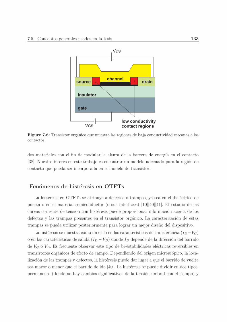
7.5. Conceptos generales usados en la tesis 133
Figure 7.6: Transistor organico que muestra las regiones de baja conductividad cercanas a loscontactos.
dos materiales con el fin de modular la altura de la barrera de energıa en el contacto
[38]. Nuestro interes en este trabajo es encontrar un modelo adecuado para la region de
contacto que pueda ser incorporada en el modelo de transistor.
Fenomenos de histeresis en OTFTs
La histeresis en OTFTs se atribuye a defectos o trampas, ya sea en el dielectrico de
puerta o en el material semiconductor (o sus interfaces) [10][40][41]. El estudio de las
curvas corriente de tension con histeresis puede proporcionar informacion acerca de los
defectos y las trampas presentes en el transistor organico. La caracterizacion de estas
trampas se puede utilizar posteriormente para lograr un mejor diseno del dispositivo.
La histeresis se muestra como un ciclo en las caracterısticas de transferencia (ID−VG)
o en las caracterısticas de salida (ID − VD) donde ID depende de la direccion del barrido
de VG o VD. Es frecuente observar este tipo de bi-estabilidades electricas reversibles en
transistores organicos de efecto de campo. Dependiendo del origen microscopico, la loca-
lizacion de las trampas y defectos, la histeresis puede dar lugar a que el barrido de vuelta
sea mayor o menor que el barrido de ida [40]. La histeresis se puede dividir en dos tipos:
permanente (donde no hay cambios significativos de la tension umbral con el tiempo) y

134 7. Resumen en espanol/Spanish summary
Intrinsic region
Depleted region
Insulator
Gate
Au AuxC L-xC
V =V ’+VDS DS C
VGS
+ + -- V ’DSVC
0
xC L
x
V
S DOrganic layer
VC
V(x)
Figure 7.7: Esquema de un perfil de potencial que se puede observar a lo largo del canal deun OTFT. Se observa una region de baja conductividad cerca de los contactos, siendo menoren la zona de drenador de acuerdo con [35].
dinamica (donde si la hay y puede ser perjudicial a la hora de querer fabricar dispositivos
estables y fiables). La permanente puede ser util en dispositivos de memoria no volatiles
(transistores de efecto campo ferroelectricos). Se han dado muchas explicaciones para
discutir el origen de la histeresis dinamica. Esta explicaciones se pueden agrupar en tres,
como se muestra en la figura. 7.8:
(i) efectos inducidos en la interfaz canal/dielectrico,
(ii) efectos inducidos por dipolos residuales (causada por la polarizacion lenta en el
dielectrico), y
(iii) los efectos de las cargas inyectadas desde el electrodo de puerta.
El mecanismo (i) se asocia a menudo con los electrones atrapados en los grupos hidro-
xilo (OH) en la interfaz canal/dielectrico [43][44][45]. El mecanismo (ii) se relaciona con

7.5. Conceptos generales usados en la tesis 135
Figure 7.8: Ilustracion de los mecanismos de histeresis: (i) canal /dielectrico interfaz inducida,(ii) la lentitud de la polarizacion inducida, y (iii) puerta de carga inducidas por inyeccionhisteresis.
grupos dipolares dentro del dielectrico, tales como los grupos hidroxilo, que pueden ser
lentamente reorientados por un campo electrico aplicado [42][44][46][47][45][48]. El me-
canismo (iii) se atribuye a los electrones que pueden ser inyectados desde electrodo de
puerta a un dielectrico y quedar atrapados en el interior del mismo [49][50]
Desafortunadamente, todos los efectos que hacen que el transistor se aleje del compor-
tamiento ideal no se muestran aislados, sino combinados entre sı. La figura. 7.9 muestra
un esquema con las caracterısticas de salida de un transistor incluyendo los efectos de
histeresis y de los contacto, y como nuestro objetivo es separar los efectos de contacto de
lo que ocurre en el canal intrınseco del transistor. La figura en la parte superior se mues-
tra el modelo de un OTFT con una zona de contacto. La figura de abajo a la izquierda
muestra las curvas de corriente-tension de un OTFT con histeresis y los fenomenos de
contacto. El uso de un modelo compacto para interpretar las caracterısticas de salida de
los OTFTs permite la separacion de las curvas de tension de corriente en el contacto y
en el canal intrınseco. El estudio de estas curvas separadas permite la determinacion de

136 7. Resumen en espanol/Spanish summary
Figure 7.9: Resumen grafico de la tesis. La figura superior se muestra el modelo de un OTFTcon una zona de contacto. La figura de abajo a la izquierda muestra las curvas de tension decorriente OTFTs con histeresis y los fenomenos de contacto. El uso de un modelo compactopara las caracterısticas de salida de OTFTs permite la separacion de las curvas de tension decorriente en el contacto y en el canal intrınseco. El estudio de estas curvas separadas permitela determinacion de la densidad de carga en el canal intrınseco y en el contacto (parte inferiorderecha). Esto conduce, finalmente, a la determinacion de la variacion de la carga atrapadadurante el ciclo de histeresis.
la densidad de carga en el canal intrınseco y en el contacto (parte inferior derecha). Esto
conduce, finalmente, a la determinacion de la variacion de la carga atrapada durante el
ciclo de histeresis. El objetivo principal de esta tesis es llevar a cabo un estudio en el que
todos estos efectos estan presentes simultaneamente.

7.6. Conclusiones 137
7.6. Conclusiones
1. Hemos hecho uso de un modelo fısico para interpretar los efectos de contacto en
transistores organicos/polimericos de lamina delgada, y lo hemos incorporado en
un modelo compacto que describe las caracterısticas de salida de estos transistores.
El modelo resultante reproduce los datos experimentales de las caracterısticas de
salida que muestran respuestas tanto lineales como respuestas altamente no lineales
en la region de bajos voltajes de drenador. Nuestro modelo se compara con otros
modelos propuestos anteriormente. Nuestro modelo proporciona una vision fısica
de la densidad de carga en la region de baja conductividad cerca del contacto y
refleja los cambios de densidad de carga en el resto del dispositivo. De hecho, la
evolucion con la tension de puerta de la densidad de carga libre en la zona del
contacto esta de acuerdo con la evolucion de la densidad de carga libre estimada
en el canal.
2. En paralelo a este modelo, se ha propuesto un procedimiento de extraccion de
parametros con el fin de determinar los parametros del modelo, incluyendo los
nuevos parametros ligados a los efectos de los contactos. Las ventajas que presen-
tan procedimientos anteriores (aunque menos precisos) se introducen en nuestro
metodo. Aunque se hacen necesarios modelos mas avanzados fısicamente, con el
fin de tener en cuenta todos los efectos que aparecen en el transistor organicos, los
modelos mas simples no puede ser descartados completamente. Hemos demostrado
su utilidad en el proceso de caracterizacion de los transistores.
3. Los diferentes pasos de nuestro procedimiento se comprueban con mediciones ex-
perimentales de transistores organicos de lamina delgada basados en Cinc Ftalo-
cianina, ası como a traves de datos de otros autores.
4. Ademas, se ha probado el metodo de caracterizacion en un transistor con parame-
tros conocidos, donde no se han obtenido errores significativos entre los parametros
reales y los extraıdos con el metodo.
5. El metodo de caracterizacion se ha aplicado tambien a otros transistores que mues-
tran histeresis en las caracterısticas de salida, ademas de tener presentes los efectos
de los contactos. Ello ha hecho que la caracterizacion de estos transistores sea mas

138 7. Resumen en espanol/Spanish summary
difıcil. Hemos presentado una tecnica, basada en el modelo compacto desarrollado
previamente, para extraer los parametros fundamentales del transistor, tales como
la movilidad de los portadores, la tension umbral y la variacion de la carga atra-
pada durante un ciclo de histeresis. La tecnica propuesta soluciona los problemas
de tener un mayor numero de parametros en el modelo, ası como el que exista una
relacion intrınseca entre algunos de estos parametros, tales como la dependencia
de la tension de umbral con la carga atrapada, especialmente a altas tensiones de
puerta.
La extraccion de curvas de corriente tension en la region de los contactos y en
el canal intrınseco a partir de las caracterısticas de salida experimentales ha per-
mitido resolver estos problemas. En particular, el estudio de la evolucion de la
densidad de carga con la tension de puerta, tanto en la region de contacto como en
el canal intrınseco, es esencial para extraer los parametros del transistor. Se han
vuelto a analizar transistores que muestran respuestas lineales y no lineales en la
zona de mas bajas tensiones en las curvas caracterısticas de salida. Los resultados
obtenidos con nuestra tecnica se han comparado con otros resultados proporciona-
dos por diferentes autores que empleaban tecnicas experimentales mas elaboradas,
encontrandose un buen acuerdo.
6. Se han presentado diferentes procedimientos para determinar la variacion de la
carga atrapada en un transistor organico durante un ciclo de histeresis. Los proce-
dimientos difieren en la forma en la que se tratan los efectos de contacto presentes
en los datos experimentales. Todos los procedimientos se basan en la separacion
de las contribuciones del transistor intrınseco y la region de contacto a partir de
los datos experimentales. Con el objeto de determinar la densidad de carga atra-
pada, se han usado tres tipos de curvas de corriente-tension: las correspondientes
al transistor intrınseco, las del transistor externo, y las de situaciones intermedias
donde los contactos se eliminan de forma parcial. Se han comparado los resultados
de forma cuantitativa.
7. Se ha hecho un estudio de los efectos de la region de contacto sobre el valor de
la movilidad extraıda usando diferentes modelos. Una extraccion correcta de la
movilidad con un modelo que incorpora los efectos de contacto es esencial para
obtener buenos resultados, incluso si se consideran las tensiones en los terminales
7.6. Conclusiones 139
externos del transistor en lugar de las tensiones en el transistor intrınseco. En este
sentido, un modelo compacto que describe las caracterısticas de salida del transistor
e incluye el efecto de las regiones de contacto se considera como el mejor escenario.
El peor escenario es cuando la tension de contacto se elimina parcialmente de las
tensiones en los terminales.
8. La interpretacion de las caracterısticas de salida con histeresis con diferentes mo-
delos muestra como los valores de la variacion de la carga trampa estan claramente
alterados por la inclusion o no de los efectos de contacto sobre las tensiones en
los terminales y la movilidad. Los valores obtenidos son siempre diferentes y mas
bajos que los obtenidos con nuestro modelo compacto. A partir de estos resultados,
se destaca la importancia de utilizar el modelo compacto que tiene en cuenta los
efectos de contacto del transistor y extrae de forma precisa la informacion de la
carga atrapada en el semiconductor durante un ciclo de histeresis.

140 7. Resumen en espanol/Spanish summary

Bibliografıa
[1] O. Marinov, M.J. Deen, and B. Iniguez. Charge transport in organic and polymer
thin-film transistors: recent issues. Circuits, Devices and Systems, IEE Proceedings,
152(3):189 – 209, June 2005.
[2] Pablo Lara Bullejos. Modelling of physical mechanisms in organic thin film transis-
tors and related structure. PhD thesis, Ph.D. dissertation, Universidad de Grana-
da. Departamento de Electronica y Tecnologia de Computadores., Granada, Spain,
2009.
[3] Gilles Horowitz, Riadh Hajlaoui, Denis Fichou, and Ahmed El Kassmi. Gate voltage
dependent mobility of oligothiophene field-effect transistors. Journal of Applied
Physics, 85(6):3202–3206, 1999.
[4] Pablo Lara Bullejos, Juan A. Jimenez Tejada, M. J. Deen, O. Marinov, and W. R.
Datars. Unified model for the injection and transport of charge in organic diodes.
Journal of Applied Physics, 103(6):064504, 2008.
[5] C. K. Chiang, C. R. Fincher, Y. W. Park, A. J. Heeger, H. Shirakawa, E. J. Louis,
S. C. Gau, and Alan G. MacDiarmid. Electrical conductivity in doped polyacetylene.
Phys. Rev. Lett., 39:1098–1101, Oct 1977.
[6] C. W. Tang and S. A. VanSlyke. Organic electroluminescent diodes. Applied Physics
Letters, 51(12):913–915, 1987.
[7] Michael L. Chabinyc, William S. Wong, Alberto Salleo, Kateri E. Paul, and Ro-
bert A. Street. Organic polymeric thin-film transistors fabricated by selective de-
wetting. Applied Physics Letters, 81(22):4260–4262, 2002.
141

142 Bibliografıa
[8] I. Kymissis, C.D. Dimitrakopoulos, and S. Purushothaman. High-performance bot-
tom electrode organic thin-film transistors. Electron Devices, IEEE Transactions
on, 48(6):1060 –1064, Jun 2001.
[9] O. Marinov, M.J. Deen, U. Zschieschang, and H. Klauk. Organic thin-film tran-
sistors: Part I. Compact dc modeling. Electron Devices, IEEE Transactions on,
56(12):2952 –2961, dec. 2009.
[10] Jae Bon Koo, Chan Hoe Ku, Sang Chul Lim, Seong Hyun Kim, and Jung Hun
Lee. Hysteresis and threshold voltage shift of pentacene thin-film transistors and
inverters with Al2O3 gate dielectric. Applied Physics Letters, 90(13):133503, 2007.
[11] R. Schroeder, L. Majewski, and M. Grell. All-organic permanent memory transistor
using an amorphous, spin-cast ferroelectric-like gate insulator. Advanced Materials,
16(7):633–636, 2004.
[12] Th. B. Singh, N. Marjanovic, G. J. Matt, N. S. Sariciftci, R. Schwodiauer, and
S. Bauer. Nonvolatile organic field-effect transistor memory element with a poly-
meric gate electret. Applied Physics Letters, 85(22):5409–5411, 2004.
[13] C. Ucurum, H. Goebel, F. A. Yildirim, W. Bauhofer, and W. Krautschneider. Ho-
le trap related hysteresis in pentacene field-effect transistors. Journal of Applied
Physics, 104(8):084501, 2008.
[14] C. Goldmann, S. Haas, C. Krellner, K. P. Pernstich, D. J. Gundlach, and B. Batlogg.
Hole mobility in organic single crystals measured by a (flip-crystal) field-effect tech-
nique. Journal of Applied Physics, 96(4):2080–2086, 2004.
[15] Howard E. Katz, Jerainne Johnson, Andrew J. Lovinger, and Wenjie Li. Naphtha-
lenetetracarboxylic diimide-based n-channel transistor semiconductors: Structural
variation and thiol-enhanced gold contacts. Journal of the American Chemical So-
ciety, 122(32):7787–7792, 2000.
[16] Zhenan Bao, Andrew J. Lovinger, and Janelle Brown. New air-stable n-channel
organic thin film transistors. Journal of the American Chemical Society, 120(1):207–
208, 1998.

Bibliografıa 143
[17] A. Facchetti, M. Mushrush, H.E. Katz, and T.J. Marks. n-type building blocks
for organic electronics: A homologous family of fluorocarbon-substituted thiophene
oligomers with high carrier mobility. Advanced Materials, 15(1):33–38, 2003.
[18] Antonio Facchetti, Yvonne Deng, Anchuan Wang, Yoshihiro Koide, Henning Sirring-
haus, Tobin J. Marks, and Richard H. Friend. Tuning the semiconducting properties
of sexithiophene by a, w-substitution-a,w-diperfluorohexylsexithiophene: The first
n-type sexithiophene for thin-film transistors. Angewandte Chemie International
Edition, 39(24):4547–4551, 2000.
[19] Patrick R. L. Malenfant, Christos D. Dimitrakopoulos, Jeffrey D. Gelorme, Laura L.
Kosbar, Teresita O. Graham, Alessandro Curioni, and Wanda Andreoni. N-type or-
ganic thin-film transistor with high field-effect mobility based on a n,n[sup [prime]]-
dialkyl-3,4,9,10-perylene tetracarboxylic diimide derivative. Applied Physics Letters,
80(14):2517–2519, 2002.
[20] HE Katz, AJ Lovinger, J Johnson, C Kloc, T Siegrist, W Li, YY Lin, and A Doda-
balapur. A soluble and air-stable organic semiconductor with high electron mobility.
NATURE, 404(6777):478–481, MAR 30 2000.
[21] Z. Bao. Materials and fabrication needs for low-cost organic transistor circuits.
Advanced Materials, 12(3):227–230, 2000.
[22] D.J. Gundlach, Li Li Jia, and T.N. Jackson. Pentacene TFT with improved li-
near region characteristics using chemically modified source and drain electrodes.
Electron Device Letters, IEEE, 22(12):571 –573, dec. 2001.
[23] P.K. Weimer. The tft a new thin-film transistor. Proceedings of the IRE, 50(6):1462
–1469, June 1962.
[24] Howard E. Katz and Jia Huang. Thin-film organic electronic devices. Annual Review
of Materials Research, 39(1):71–92, 2009.
[25] Gilles Horowitz and Philippe Delannoy. An analytical model for organic-based thin-
film transistors. Journal of Applied Physics, 70(1):469–475, 1991.
[26] P. Murgatroyd. Theory of space-charge-limited current enhanced by Frenkel effect.
Journal of Physics D: Applied Physics, 3(2):151, 1970.

144 Bibliografıa
[27] A. Lodha and R. Singh. Prospects of manufacturing organic semiconductor-based
integrated circuits. Semiconductor Manufacturing, IEEE Transactions on, 14(3):281
–296, aug 2001.
[28] G. Ghibaudo, O. Roux, Ch. Nguyen-Duc, F. Balestra, and J. Brini. Improved
analysis of low frequency noise in field-effect mos transistors. physica status solidi
(a), 124(2):571–581, 1991.
[29] O Marinov, MJ Deen, J Yu, G Vamvounis, S Holdcroft, and W Woods. Low-
frequency noise in polymer thin-film transistors. IEE Procedings-Circuits Devices
and Systems, 151(5):466–472, Oct 2004.
[30] Gilles Horowitz, Xuezhou Peng, Denis Fichou, and Francis Garnier. The
oligothiophene-based field-effect transistor: How it works and how to improve it.
Journal of Applied Physics, 67(1):528–532, 1990.
[31] Gilles Horowitz, Mohsen E. Hajlaoui, and Riadh Hajlaoui. Temperature and ga-
te voltage dependence of hole mobility in polycrystalline oligothiophene thin film
transistors. Journal of Applied Physics, 87(9):4456–4463, 2000.
[32] Gilles Horowitz. Organic thin film transistors: From theory to real devices. Journal
of Materials Research, 19:1946–1962.
[33] Vissenberg M and Matters M. Theory of the field-effect mobility in amorphous
organic transistors. Phys. Rev. B, 57:12964, 1998.
[34] C. D. Dimitrakopoulos, I. Kymissis, S. Purushothaman, D. A. Neumayer, P. R.
Duncombe, and R. B. Laibowitz. Low-voltage, high-mobility pentacene transistors
with solution-processed high dielectric constant insulators. Advanced Materials,
11(16):1372–1375, 1999.
[35] L. Burgi, T. J. Richards, R. H. Friend, and H. Sirringhaus. Close look at char-
ge carrier injection in polymer field-effect transistors. Journal of Applied Physics,
94(9):6129–6137, 2003.
[36] P. Lara Bullejos, J. A. Jimenez Tejada, S. Rodrıguez-Bolivar, M. J. Deen, and
O. Marinov. Model for the injection of charge through the contacts of organic
transistors. Journal of Applied Physics, 105(8):084516, 2009.

Bibliografıa 145
[37] Dipti Gupta, Namho Jeon, and Seunghyup Yoo. Modeling the electrical characteris-
tics of tips-pentacene thin-film transistors: Effect of contact barrier, field-dependent
mobility, and traps. Organic Electronics, 9(6):1026 – 1031, 2008.
[38] I. H. Campbell, S. Rubin, T. A. Zawodzinski, J. D. Kress, R. L. Martin, D. L. Smith,
N. N. Barashkov, and J. P. Ferraris. Controlling schottky energy barriers in orga-
nic electronic devices using self-assembled monolayers. Phys. Rev. B, 54:R14321–
R14324, Nov 1996.
[39] R. A. Street and A. Salleo. Contact effects in polymer transistors. Applied Physics
Letters, 81(15):2887–2889, 2002.
[40] Martin Egginger, Siegfried Bauer, Reinhard Schwoediauer, Helmut Neugebauer, and
Niyazi Serdar Sariciftci. Current versus gate voltage hysteresis in organic field effect
transistors. Monatshefte Fur Chemie, 140(7):735–750, Jul 2009.
[41] C. S. Fuller and J. C. Severiens. Mobility of impurity ions in germanium and silicon.
Phys. Rev., 96:21–24, Oct 1954.
[42] H. Klauk. Organic Electronics. Wiley, Weinheim, 2006.
[43] Gong Gu, Michael G. Kane, James E. Doty, and Arthur H. Firester. Electron traps
and hysteresis in pentacene-based organic thin-film transistors. Applied Physics
Letters, 87(24):243512, 2005.
[44] Gong Gu, Michael G. Kane, and Siun-Chuon Mau. Reversible memory effects and
acceptor states in pentacene-based organic thin-film transistors. Journal of Applied
Physics, 101(1):014504, 2007.
[45] D. K. Hwang, Kimoon Lee, Jae Hoon Kim, Seongil Im, Ji Hoon Park, and Eugene
Kim. Comparative studies on the stability of polymer versus sio2 gate dielectrics
for pentacene thin-film transistors. Applied Physics Letters, 89(9):093507, 2006.
[46] Howard E. Katz, X. Michael Hong, Ananth Dodabalapur, and Rahul Sarpeshkar.
Organic field-effect transistors with polarizable gate insulators. Journal of Applied
Physics, 91(3):1572–1576, 2002.

146 Bibliografıa
[47] Taeho Jung, Ananth Dodabalapur, Robert Wenz, and Siddharth Mohapatra. Mois-
ture induced surface polarization in a poly(4-vinyl phenol) dielectric in an organic
thin-film transistor. Applied Physics Letters, 87(18):182109, 2005.
[48] Sang Chul Lim, Seong Hyun Kim, Jae Bon Koo, Jung Hun Lee, Chan Hoe Ku,
Yong Suk Yang, and Taehyoung Zyung. Hysteresis of pentacene thin-film transistors
and inverters with cross-linked poly(4-vinylphenol) gate dielectrics. Applied Physics
Letters, 90(17):173512, 2007.
[49] D. K. Hwang, J. H. Park, J. Lee, J. M. Choi, J. H. Kim, E. Kim, and J. S. Im.
Electrochem. Soc. 8, G24, 2006.
[50] Cheon An Lee, Dong-Wook Park, Keum-Dong Jung, Byung ju Kim, Yoo Chul Kim,
Jong Duk Lee, and Byung-Gook Park. Hysteresis mechanism in pentacene thin-
film transistors with poly(4-vinyl phenol) gate insulator. Applied Physics Letters,
89(26):262120, 2006.
[51] Se Hyun Kim, Hoichang Yang, Sang Yoon Yang, Kipyo Hong, Danbi Choi, Chanwoo
Yang, Dae Sung Chung, and Chan Eon Park. Effect of water in ambient air on
hysteresis in pentacene field-effect transistors containing gate dielectrics coated with
polymers with different functional groups. Organic Electronics, 9(5):673 – 677, 2008.
[52] Qingshuo Wei, Keisuke Tajima, and Kazuhito Hashimoto. Electrical instability of
polymer thin-film transistors using contact film transfer methods. Applied Physics
Letters, 96(24):243301, 2010.
[53] M. Coll, K. P. Goetz, B. R. Conrad, C. A. Hacker, D. J. Gundlach, C. A. Richter,
and O. D. Jurchescu. Flip chip lamination to electrically contact organic single
crystals on flexible substrates. Applied Physics Letters, 98(16):163302, 2011.
[54] Antonio Facchetti. pi-conjugated polymers for organic electronics and photovoltaic
cell applications. Chemistry of Materials, 23(3):733–758, 2011.
[55] S. C. Jain, W. Geens, A. Mehra, V. Kumar, T. Aernouts, J. Poortmans, R. Mertens,
and M. Willander. Injection- and space charge limited-currents in doped conducting
organic materials. Journal of Applied Physics, 89(7):3804–3810, 2001.

Bibliografıa 147
[56] D. J. Gundlach, L. Zhou, J. A. Nichols, T. N. Jackson, P. V. Necliudov, and M. S.
Shur. An experimental study of contact effects in organic thin film transistors.
Journal of Applied Physics, 100(2):024509, 2006.
[57] B. H. Hamadani, C. A. Richter, D. J. Gundlach, R. J. Kline, I. McCulloch, and
M. Heeney. Influence of source-drain electric field on mobility and charge transport
in organic field-effect transistors. Journal of Applied Physics, 102(4):044503, 2007.
[58] S. Haas, A. F. Stassen, G. Schuck, K. P. Pernstich, D. J. Gundlach, B. Batlogg,
U. Berens, and H.-J. Kirner. High charge-carrier mobility and low trap density in a
rubrene derivative. Phys. Rev. B, 76:115203, Sep 2007.
[59] B.H. Hamadani and D. Natelson. Extracting contact effects in organic fets. Procee-
dings of the IEEE, 93(7):1306 –1311, july 2005.
[60] B. H. Hamadani and D. Natelson. Gated nonlinear transport in organic polymer
field effect transistors. Journal of Applied Physics, 95(3):1227–1232, 2004.
[61] E. J. Meijer, G. H. Gelinck, E. van Veenendaal, B.-H. Huisman, D. M. de Leeuw,
and T. M. Klapwijk. Scaling behavior and parasitic series resistance in disordered
organic field-effect transistors. Applied Physics Letters, 82(25):4576–4578, 2003.
[62] P. V. Necliudov, M. S. Shur, D. J. Gundlach, and T. N. Jackson. Modeling of organic
thin film transistors of different designs. Journal of Applied Physics, 88(11):6594–
6597, 2000.
[63] P. Lara Bullejos, J. A. Jimenez Tejada, F. M. Gomez-Campos, M. J. Deen, and
O. Marinov. Evaluation of the charge density in the contact region of organic thin
film transistors. Journal of Applied Physics, 106(9):094503, 2009.
[64] Mahmut Durmus, Colette Lebrun, and Vefa Ahsen. Synthesis and characterization
of novel liquid and liquid crystalline phthalocyanines. Journal of Porphyrins and
Phthalocyanines, 08(10):1175–1186, 2004.
[65] Weiying Gao and Antoine Kahn. Controlled p-doping of zinc phthalocyanine by
coevaporation with tetrafluorotetracyanoquinodimethane: A direct and inverse pho-
toemission study. Applied Physics Letters, 79(24):4040–4042, 2001.

148 Bibliografıa
[66] Z. Xie, M. S. A. Abdou, X. Lu, M. J. Deen, and S. Holdcroft. Electrical characte-
ristics and photolytic tuning of poly (3-lhexylthiophene) thin film metal- insulator-
semiconductor field- effect transistors (misfets). Canadian Journal of Physics, 70(10-
11):1171–1177, Oct-Nov 1992. 6Th Canadian Semiconductor Technology Conf, Ot-
tawa, Canada, Aug, 1992.
[67] M. Jamal Deen, Mehdi H. Kazemeini, and S. Holdcroft. Contact effects and extrac-
tion of intrinsic parameters in poly(3-alkylthiophene) thin film field-effect transis-
tors. Journal of Applied Physics, 103(12):124509, 2008.
[68] M. Shur and M. Hack. Physics of amorphous silicon based alloy field-effect transis-
tors. Journal of Applied Physics, 55(10):3831–3842, 1984.
[69] M. C. J. M. Vissenberg and M. J. M. de Jong. Theory of electric-field-induced
photoluminescence quenching in disordered molecular solids. Phys. Rev. B, 57:2667–
2670, Feb 1998.
[70] E. Calvetti, A. Savio, Zs. M. Kovacs-Vajna, and L. Colalongo. Analytical model for
organic thin-film transistors operating in the subthreshold region. Applied Physics
Letters, 87(22):223506, 2005.
[71] O. Marinov, M. J. Deen, and R. Datars. Compact modeling of charge carrier mobility
in organic thin-film transistors. Journal of Applied Physics, 106(6):064501, 2009.
[72] M.J. Deen, O. Marinov, U. Zschieschang, and H. Klauk. Organic thin-film tran-
sistors: Part ii ;parameter extraction. Electron Devices, IEEE Transactions on,
56(12):2962 –2968, dec. 2009.
[73] A. Cerdeira, M. Estrada, R. Garcia, A. Ortiz Conde, and F.J. Garcia Sanchez. New
procedure for the extraction of basic a-si:h tft model parameters in the linear and
saturation regions. Solid-State Electronics, 45(7):1077 – 1080, 2001.
[74] K. Tsukagoshi, F. Fujimori, T. Minari, T. Miyadera, T. Hamano, and Y. Aoyagi.
Suppression of short channel effect in organic thin film transistors. Applied Physics
Letters, 91(11):113508, 2007.
[75] B. H. Hamadani and D. Natelson. Nonlinear charge injection in organic field-effect
transistors. Journal of Applied Physics, 97(6):064508, 2005.

Bibliografıa 149
[76] D Chirvase, Z Chiguvare, M Knipper, J Parisi, V Dyakonov, and JC Hummelen.
Temperature dependent characteristics of poly(3 hexylthiophene)-fullerene based
heterojunction organic solar cells. Journal of Applied Physics, 93(6):3376–3383,
Mar 15 2003.
[77] B. G. Streetman. Solid State Electronic Devices. Prentice-Hall, Englewood Cliffs,
NJ, 1980.
[78] Mohamed S. A. Abdou, Xiaotang Lu, Zi W. Xie, Frank Orfino, M. Jamal Deen,
and Steven Holdcroft. Nature of impurities in .pi.-conjugated polymers prepared
by ferric chloride and their effect on the electrical properties of metal-insulator-
semiconductor structures. Chemistry of Materials, 7(4):631–641, Apr 1995.
[79] Mohamed S. A. Abdou, Frank P. Orfino1, Zi W. Xie, M. Jamal Deen, and Steven
Holdcroft. Reversible charge transfer complexes between molecular oxygen and
poly(3-alkylthiophene)s. Advanced Materials, 6(11):838–841, Nov 1994.
[80] O. Marinov, M. J. Deen, B. Iniguez, and B. Ong. Charge localization in polymeric
metal-oxide-semiconductor capacitors. Journal of Vacuum Science Technology A:
Vacuum, Surfaces, and Films, 24(3):649 –653, may 2006.
[81] Gong Gu and Michael G. Kane. Moisture induced electron traps and hysteresis in
pentacene-based organic thin-film transistors. Applied Physics Letters, 92(5):053305,
2008.
[82] D. K. Hwang, Min Suk Oh, Jung Min Hwang, Jae Hoon Kim, and Seongil Im.
Hysteresis mechanisms of pentacene thin-film transistors with polymer/oxide bilayer
gate dielectrics. Applied Physics Letters, 92(1):013304, 2008.
[83] J.A. Jimenez Tejada, K.M. Awawdeh, J.A. Lopez Villanueva, J.E. Carceller, M.J.
Deen, N.B. Chaure, Tamara Basova, and A.K. Ray. Contact effects in compact
models of organic thin film transistors: Application to zinc phthalocyanine-based
transistors. Organic Electronics, 12(5):832 – 842, 2011.
[84] C. Petit, D. Zander, K. Lmimouni, M. Ternisien, D. Tondelier, S. Lenfant, and
D. Vuillaume. Gate pulse electrical method to characterize hysteresis phenomena
in organic field effect transistor. Organic Electronics, 9(6):979 – 984, 2008.

150 Bibliografıa
[85] Jeong Ho Cho, Jung Ah Lim, Joong Tark Han, Ho Won Jang, Jong-Lam Lee, and
Kilwon Cho. Control of the electrical and adhesion properties of metal/organic
interfaces with self-assembled monolayers. Applied Physics Letters, 86(17):171906,
2005.
[86] K.M. Awawdeh, J.A.J. Tejada, J.A.L. Villanueva, J.E. Carceller, M.J. Deen, N.B.
Chaure, T. Basova, and A.K. Ray. Compact modeling of the contact effects in
organic thin film transistors. In Electron Devices (CDE), 2011 Spanish Conference
on, pages 1 –4, feb. 2011.
[87] Martin Egginger. Electrical Characterisation of Poly(vinyl alcohol) based Organic
Field Effect Transistors. PhD thesis, Ph.D. dissertation, Johannes Kepler University
of Linz, Johannes Kepler University Linz, AltenbergerstraBe, Linz, Austria, 2009.
[88] M.J. Deen, O. Marinov, S. Holdcroft, and W. Woods. Low-frequency noise in poly-
mer transistors. Electron Devices, IEEE Transactions on, 48(8):1688 –1695, aug
2001.
[89] M.J. Deen, M.H. Kazemeini, Y.M. Haddara, Jianfei Yu, G. Vamvounis, S. Hold-
croft, and W. Woods. Electrical characterization of polymer-based fets fabricated
by spin-coating poly(3-alkylthiophene)s. Electron Devices, IEEE Transactions on,
51(11):1892 – 1901, nov. 2004.
[90] P. Lopez Varo, J.A. Jimenez Tejada, J.A. Lopez Villanueva, J.E. Carceller, and M.J.
Deen. Modeling the transition from ohmic to space charge limited current in organic
semiconductors. Organic Electronics, 13(9):1700 – 1709, 2012.
[91] K. M. Awawdeh, J. A. Jimenez Tejada, P. Lopez Varo, J. A. Lopez Villanueva,
F. M. Gomez Campos, and M. J. Deen. Characterization of organic thin film tran-
sistors with hysteresis and contact effects. Organic Electronics, x(x):x, 2013.
[92] Peter V Necliudov, Michael S Shur, David J Gundlach, and Thomas N Jackson.
Contact resistance extraction in pentacene thin film transistors. Solid-State Elec-
tronics, 47(2):259 – 262, 2003.

Appendix I
Publicaciones.
151

152 Appendix I. Publicaciones.
Publicaciones a fecha de entrega en la Escuela de Posgrado de la Universidad de
Granada:
Journal publications
a) Contact effects in compact models of organic thin film transistors:
application to zinc phthalocyanine-based transistors. J. A. Jimenez Te-
jada, K. M. Awawdeh, J. A. Lopez Villanueva, J. E. Carceller, M. J. Deen, N. B.
Chaure, T. Basova, and A. K. Ray. Organic Electronics 2011.
b) Characterization of organic thin film transistors with hysteresis and
contact effects. K. M. Awawdeh, J. A. Jimenez Tejada, P. Lopez Varo, J. A.
Lopez Villanueva, F. M. Gomez Campos, and M. J. Deen. Organic Electronics 2013,
submitted.
c) Determination of the variation of the trapped charge in organic thin
film transistors during hysteresis. K. M. Awawdeh, J. A. Jimenez Tejada, P.
Lopez Varo, J. A. Lopez Villanueva, M. J. Deen. 2013, In preparation.
Conference publications
d) Invited paper. Towards a compact model for the injection of char-
ge into organic/polymeric semiconductors. J. A. Jimenez Tejada, L. Puga
Pedregosa, K. M. Awawdeh, M. J. Deen. ISFE’10-3rd International Symposium on
Flexible electronics, Meeting Abstracts, 2010.
e) Compact modeling of the contact effects in organic thin film transis-
tors. K. M. Awawdeh, J. A. Jimenez Tejada, J. A. Lopez Villanueva, J. E. Carceller,
M. J. Deen, N. B. Chaure, T. Basova, and A. K.Ray. IEEE Proceedings of the 8th
Spanish Conference on Electron Devices, CDE’2011, , 2011.
f) Invited paper. Contact effects and hysteresis in organic thin film
transistors J. A. Jimenez Tejada, K. M. Awawdeh, P. Lopez Varo, A. K.Ray,
M. J. Deen. ECS-219th Electrochemical Society, Meeting Abstracts, 2011.

153
g) Study of electrical phenomena in organic devices: solar cells, diodes,
thin film transistors P. Lopez Varo, K. M. Awawdeh, J. A. Jimenez Tejada. 4th
EMUNI Research Souk the Euro-Mediterranean Student Research Multi-Conference,
Meeting Abstracts, 2012.
h) Method of extraction of mobility model parameters in organic diodes
P. Lopez Varo, J. A. Jimenez Tejada, J. A. Lopez Villanueva, K. M. Awawdeh, M.
J. Deen. ICOE 2012-8th International Conference on Organic Electronics, Meeting
Abstracts, 2012.
i) Influence of the contact effects on the variation of the trapped
charge in the intrinsic channel of organic thin film transistors. K. M.
Awawdeh, J. A. Jimenez Tejada, P. Lopez Varo, J. A. Lopez Villanueva, M. J. Deen.
IEEE Proceedings of the 9th Spanish Conference on Electron Devices, CDE’2013, ,
2013.
j) Invited paper. Modeling of charge injection in organic/polymeric dio-
des J. A. Jimenez Tejada, P. Lopez Varo, K. M. Awawdeh, M. J. Deen. ECS-223th
Electrochemical Society, Meeting Abstracts, 2013.
k) Monitoring the introduction of impurities in organic/polymeric diodes
by the analysis of current voltage curves P. Lopez Varo, J. A. Jimenez
Tejada, K. M. Awawdeh, M. J. Deen. ICOE 2013-9th International Conference on
Organic Electronics, Meeting Abstracts, 2013.

154 Appendix I. Publicaciones.


![Journal of Arrhythmia - COnnecting REpositories · of arrhythmia diagnosis [1], and implantable loop recorders are especially suitable for identifying undetected sources of a suspected](https://static.fdocuments.mx/doc/165x107/607210056cc22557db7f5efd/journal-of-arrhythmia-connecting-repositories-of-arrhythmia-diagnosis-1-and.jpg)