3. Diodos de unión p-n 4. El MOSFETyolotli.inaoep.mx/portalfiles/AplicacionesDiodo.pdf · Curso...
22
Curso propedéutico de Electrónica INAOE 2009 Dr. Pedro Rosales Quintero 95 3. Diodos de unión p-n 3.1 Diodo de unión p-n 3.2 Diodos túnel 3.3 Fotodiodos 3.4 LEDs y láseres 3.5 Transistor Bipolar de unión 4. El MOSFET 41 El capacitor MOS ideal 4.2 Efectos en superficies reales 4.3 Voltaje de encendido 4.4 Operación básica del transistor MOS 4.5 Control del voltaje de encendido 4.6 Fabricación del MOS Curso propedéutico de Electrónica INAOE 2009 Dr. Pedro Rosales Quintero 96 p-n Junction Diodes The diodes are designed to exploit specific junctions properties. Rectifiers The most obvious property of a p-n junction is its unilateral nature; that this, to a good approximation its conducts current in only one direction.
Transcript of 3. Diodos de unión p-n 4. El MOSFETyolotli.inaoep.mx/portalfiles/AplicacionesDiodo.pdf · Curso...
Curso propedéutico de Electrónica INAOE 2009 Dr. Pedro Rosales Quintero 95
3. Diodos de unión p-n
3.1 Diodo de unión p-n
3.2 Diodos túnel
3.3 Fotodiodos
3.4 LEDs y láseres
3.5 Transistor Bipolar de unión
4. El MOSFET
41 El capacitor MOS ideal
4.2 Efectos en superficies reales
4.3 Voltaje de encendido
4.4 Operación básica del transistor MOS
4.5 Control del voltaje de encendido
4.6 Fabricación del MOS
Curso propedéutico de Electrónica INAOE 2009 Dr. Pedro Rosales Quintero 96
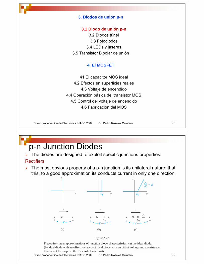
p-n Junction DiodesThe diodes are designed to exploit specific junctions properties.
Rectifiers
The most obvious property of a p-n junction is its unilateral nature; that this, to a good approximation its conducts current in only one direction.
Curso propedéutico de Electrónica INAOE 2009 Dr. Pedro Rosales Quintero 97
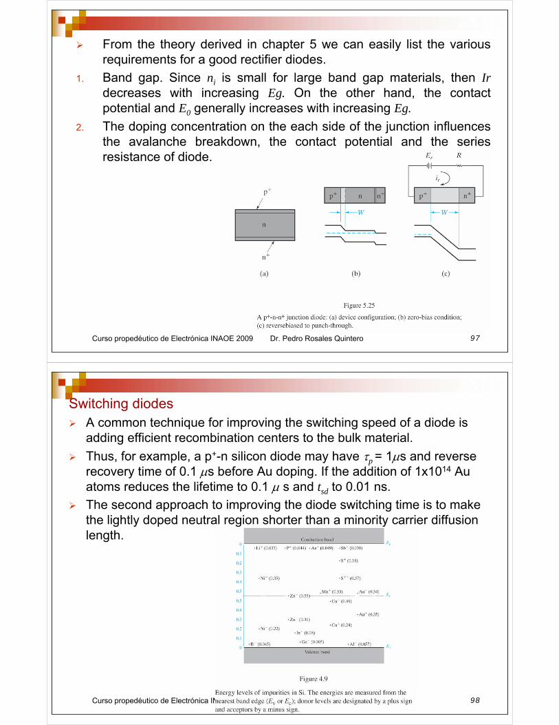
From the theory derived in chapter 5 we can easily list the various requirements for a good rectifier diodes.
1. Band gap. Since ni is small for large band gap materials, then Irdecreases with increasing Eg. On the other hand, the contact potential and E0 generally increases with increasing Eg.
2. The doping concentration on the each side of the junction influences the avalanche breakdown, the contact potential and the series resistance of diode.
Curso propedéutico de Electrónica INAOE 2009 Dr. Pedro Rosales Quintero 98
Switching diodesA common technique for improving the switching speed of a diode is adding efficient recombination centers to the bulk material.
Thus, for example, a p+-n silicon diode may have τp = 1µs and reverse recovery time of 0.1 µs before Au doping. If the addition of 1x10¹⁴ Au atoms reduces the lifetime to 0.1 µ s and tsd to 0.01 ns.
The second approach to improving the diode switching time is to make the lightly doped neutral region shorter than a minority carrier diffusion length.
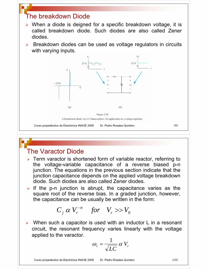
Curso propedéutico de Electrónica INAOE 2009 Dr. Pedro Rosales Quintero 99
The breakdown DiodeWhen a diode is deigned for a specific breakdown voltage, it is called breakdown diode. Such diodes are also called Zenerdiodes.
Breakdown diodes can be used as voltage regulators in circuits with varying inputs.
Curso propedéutico de Electrónica INAOE 2009 Dr. Pedro Rosales Quintero 100
The Varactor DiodeTerm varactor is shortened form of variable reactor, referring to the voltage-variable capacitance of a reverse biased p-njunction. The equations in the previous section indicate that the junction capacitance depends on the applied voltage breakdown diode. Such diodes are also called Zener diodes. If the p-n junction is abrupt, the capacitance varies as the square root of the reverse bias. In a graded junction, however, the capacitance can be usually be written in the form:
0VVforVC rn
rj >>−α
When such a capacitor is used with an inductor L in a resonant circuit, the resonant frequency varies linearly with the voltageapplied to the varactor.
rr VLC
αω 1=
Curso propedéutico de Electrónica INAOE 2009 Dr. Pedro Rosales Quintero 101
3. Diodos de unión p-n
3.1 Diodo de unión p-n
3.2 Diodos túnel
3.3 Fotodiodos
3.4 LEDs y láseres
3.5 Transistor Bipolar de unión
4. El MOSFET
41 El capacitor MOS ideal
4.2 Efectos en superficies reales
4.3 Voltaje de encendido
4.4 Operación básica del transistor MOS
4.5 Control del voltaje de encendido
4.6 Fabricación del MOS
Curso propedéutico de Electrónica INAOE 2009 Dr. Pedro Rosales Quintero 102
Degenerated SemiconductorsIf the conduction band electron concentrations n exceeds the effective density of states Nc, the Fermi level is no longer within the band gap but lies within the conduction band. When this occurs, the material is called degenerate n-typeThe analog case of degenerate p-type material occurs when the acceptor concentration is very high and the Fermi level lies in the valence band.
Curso propedéutico de Electrónica INAOE 2009 Dr. Pedro Rosales Quintero 103
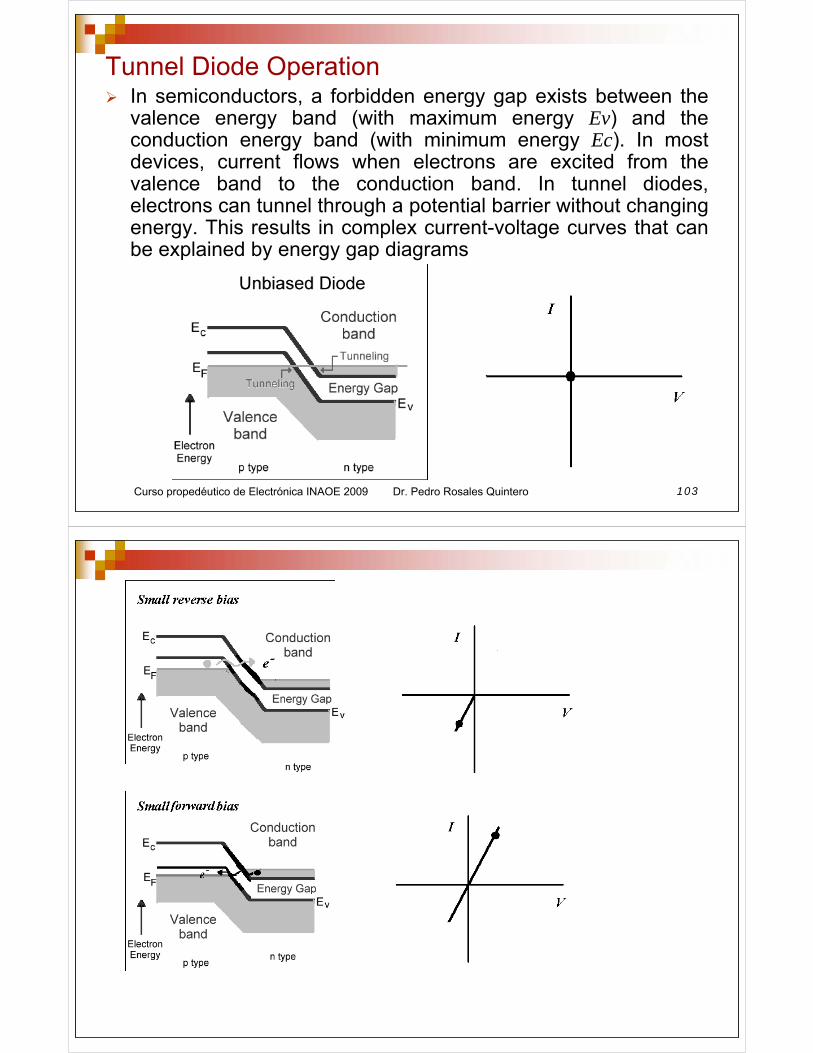
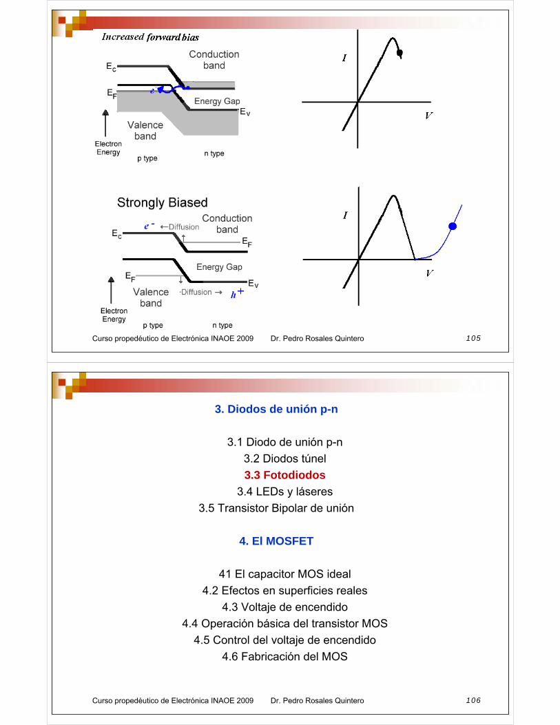
Tunnel Diode OperationIn semiconductors, a forbidden energy gap exists between the valence energy band (with maximum energy Ev) and the conduction energy band (with minimum energy Ec). In most devices, current flows when electrons are excited from the valence band to the conduction band. In tunnel diodes, electrons can tunnel through a potential barrier without changing energy. This results in complex current-voltage curves that can be explained by energy gap diagrams
Curso propedéutico de Electrónica INAOE 2009 Dr. Pedro Rosales Quintero 104
Curso propedéutico de Electrónica INAOE 2009 Dr. Pedro Rosales Quintero 105
Curso propedéutico de Electrónica INAOE 2009 Dr. Pedro Rosales Quintero 106
3. Diodos de unión p-n
3.1 Diodo de unión p-n
3.2 Diodos túnel
3.3 Fotodiodos
3.4 LEDs y láseres
3.5 Transistor Bipolar de unión
4. El MOSFET
41 El capacitor MOS ideal
4.2 Efectos en superficies reales
4.3 Voltaje de encendido
4.4 Operación básica del transistor MOS
4.5 Control del voltaje de encendido
4.6 Fabricación del MOS
Curso propedéutico de Electrónica INAOE 2009 Dr. Pedro Rosales Quintero 107
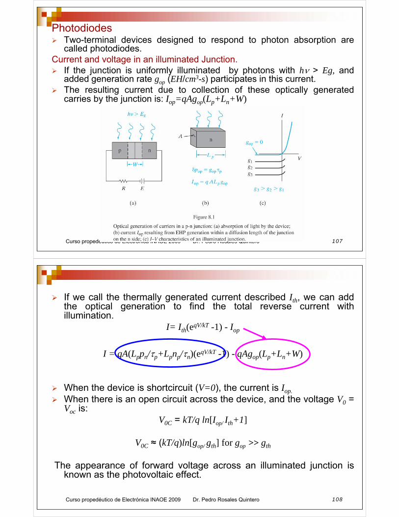
Photodiodes Two-terminal devices designed to respond to photon absorption are called photodiodes.
Current and voltage in an illuminated Junction.If the junction is uniformly illuminated by photons with hν > Eg, and added generation rate gop (EH/cm3-s) participates in this current.The resulting current due to collection of these optically generated carries by the junction is: Iop=qAgop(Lp+Ln+W)
Curso propedéutico de Electrónica INAOE 2009 Dr. Pedro Rosales Quintero 108
If we call the thermally generated current described Ith, we can add the optical generation to find the total reverse current with illumination.
I= Ith(eqV/kT -1) - Iop
I = qA(Lppn/τp+Lpnp/τn)(eqV/kT -1) - qAgop(Lp+Ln+W)
When the device is shortcircuit (V=0), the current is Iop.
When there is an open circuit across the device, and the voltage V0 = Voc is:
V0C = kT/q ln[Iop/ Ith+1]
V0C ≈ (kT/q)ln[gop/ gth] for gop >> gth
The appearance of forward voltage across an illuminated junction is known as the photovoltaic effect.
Curso propedéutico de Electrónica INAOE 2009 Dr. Pedro Rosales Quintero 109
Curso propedéutico de Electrónica INAOE 2009 Dr. Pedro Rosales Quintero 110
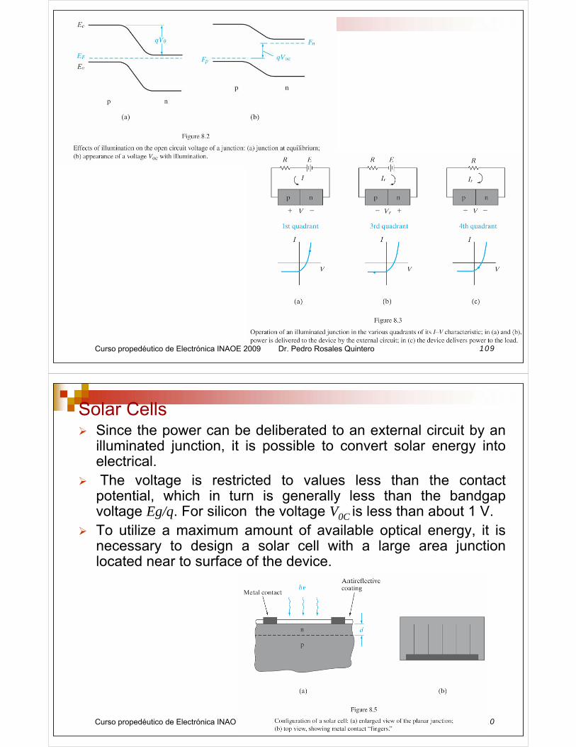
Solar CellsSince the power can be deliberated to an external circuit by an illuminated junction, it is possible to convert solar energy into electrical.The voltage is restricted to values less than the contact
potential, which in turn is generally less than the bandgapvoltage Eg/q. For silicon the voltage V0C is less than about 1 V.To utilize a maximum amount of available optical energy, it is necessary to design a solar cell with a large area junction located near to surface of the device.
Curso propedéutico de Electrónica INAOE 2009 Dr. Pedro Rosales Quintero 111
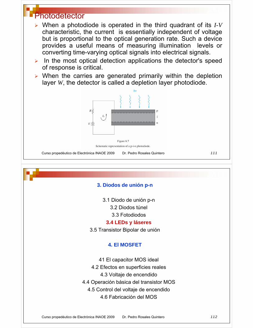
PhotodetectorWhen a photodiode is operated in the third quadrant of its I-V characteristic, the current is essentially independent of voltage but is proportional to the optical generation rate. Such a device provides a useful means of measuring illumination levels or converting time-varying optical signals into electrical signals.In the most optical detection applications the detector's speedof response is critical.When the carries are generated primarily within the depletion layer W, the detector is called a depletion layer photodiode.
Curso propedéutico de Electrónica INAOE 2009 Dr. Pedro Rosales Quintero 112
3. Diodos de unión p-n
3.1 Diodo de unión p-n
3.2 Diodos túnel
3.3 Fotodiodos
3.4 LEDs y láseres
3.5 Transistor Bipolar de unión
4. El MOSFET
41 El capacitor MOS ideal
4.2 Efectos en superficies reales
4.3 Voltaje de encendido
4.4 Operación básica del transistor MOS
4.5 Control del voltaje de encendido
4.6 Fabricación del MOS
Curso propedéutico de Electrónica INAOE 2009 Dr. Pedro Rosales Quintero 113
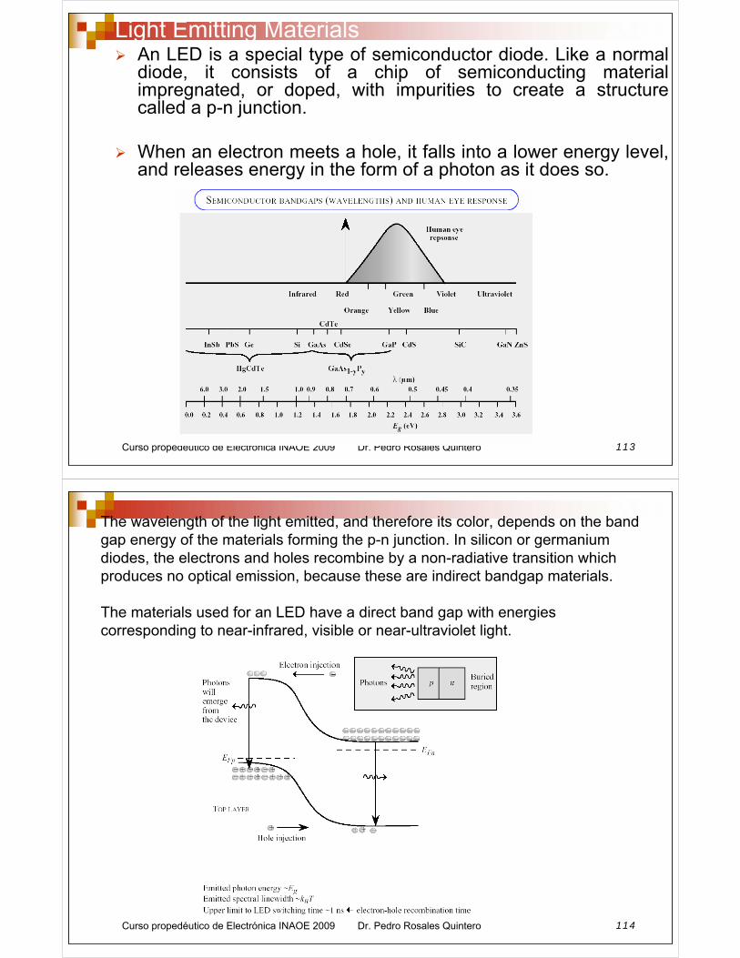
Light Emitting MaterialsAn LED is a special type of semiconductor diode. Like a normal diode, it consists of a chip of semiconducting material impregnated, or doped, with impurities to create a structure called a p-n junction.
When an electron meets a hole, it falls into a lower energy level, and releases energy in the form of a photon as it does so.
Curso propedéutico de Electrónica INAOE 2009 Dr. Pedro Rosales Quintero 114
The wavelength of the light emitted, and therefore its color, depends on the band gap energy of the materials forming the p-n junction. In silicon or germanium diodes, the electrons and holes recombine by a non-radiative transition which produces no optical emission, because these are indirect bandgap materials.
The materials used for an LED have a direct band gap with energies corresponding to near-infrared, visible or near-ultraviolet light.
Curso propedéutico de Electrónica INAOE 2009 Dr. Pedro Rosales Quintero 115
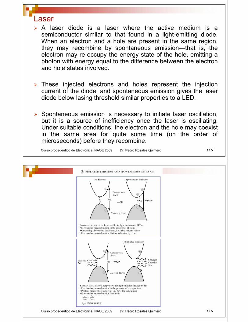
Laser A laser diode is a laser where the active medium is a semiconductor similar to that found in a light-emitting diode. When an electron and a hole are present in the same region, they may recombine by spontaneous emission—that is, the electron may re-occupy the energy state of the hole, emitting a photon with energy equal to the difference between the electron and hole states involved.
These injected electrons and holes represent the injection current of the diode, and spontaneous emission gives the laser diode below lasing threshold similar properties to a LED.
Spontaneous emission is necessary to initiate laser oscillation,but it is a source of inefficiency once the laser is oscillating. Under suitable conditions, the electron and the hole may coexistin the same area for quite some time (on the order of microseconds) before they recombine.
Curso propedéutico de Electrónica INAOE 2009 Dr. Pedro Rosales Quintero 116
Curso propedéutico de Electrónica INAOE 2009 Dr. Pedro Rosales Quintero 117
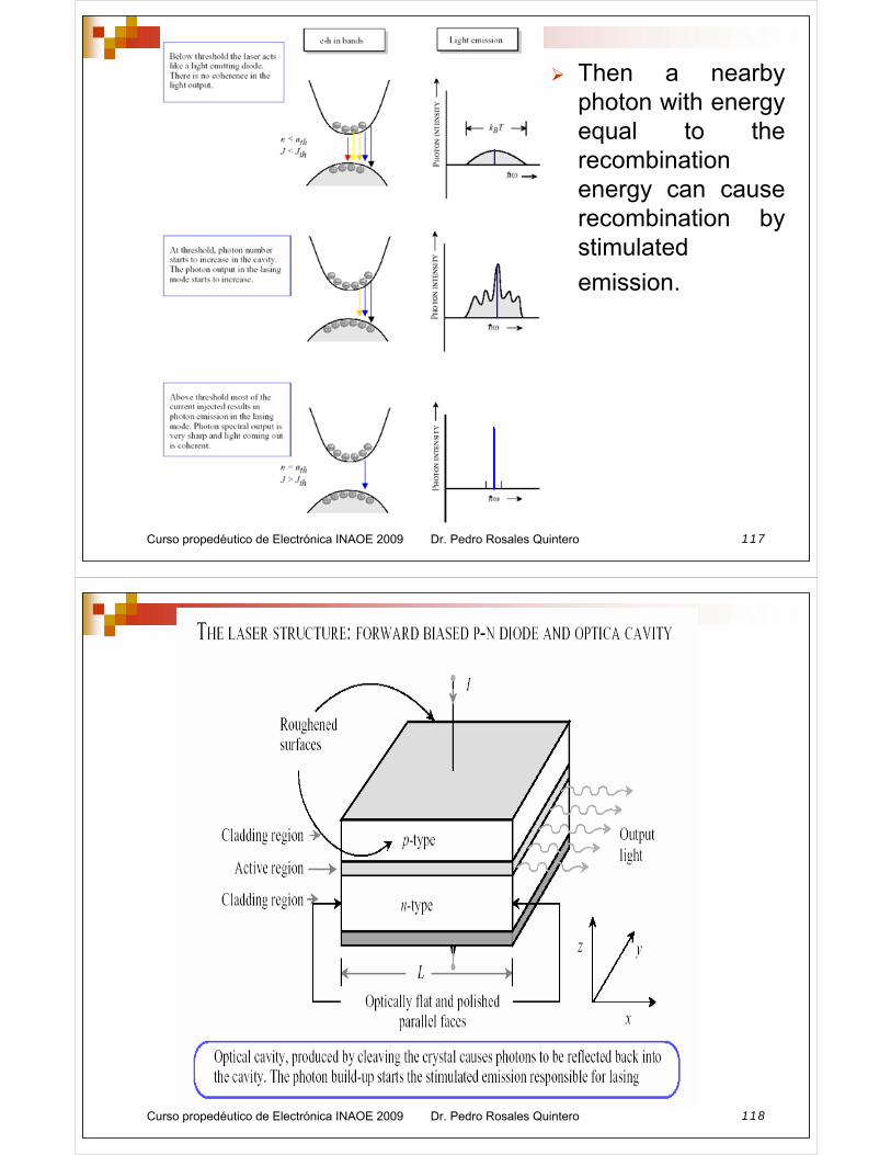
Then a nearby photon with energy equal to the recombination energy can cause recombination by stimulated
emission.
Curso propedéutico de Electrónica INAOE 2009 Dr. Pedro Rosales Quintero 118
Curso propedéutico de Electrónica INAOE 2009 Dr. Pedro Rosales Quintero 119
3. Diodos de unión p-n
3.1 Diodo de unión p-n
3.2 Diodos túnel
3.3 Fotodiodos
3.4 LEDs y láseres
3.5 Transistor Bipolar de unión
4. El MOSFET
41 El capacitor MOS ideal
4.2 Efectos en superficies reales
4.3 Voltaje de encendido
4.4 Operación básica del transistor MOS
4.5 Control del voltaje de encendido
4.6 Fabricación del MOS
120Curso propedéutico de Electrónica INAOE 2009 Dr. Pedro Rosales Quintero
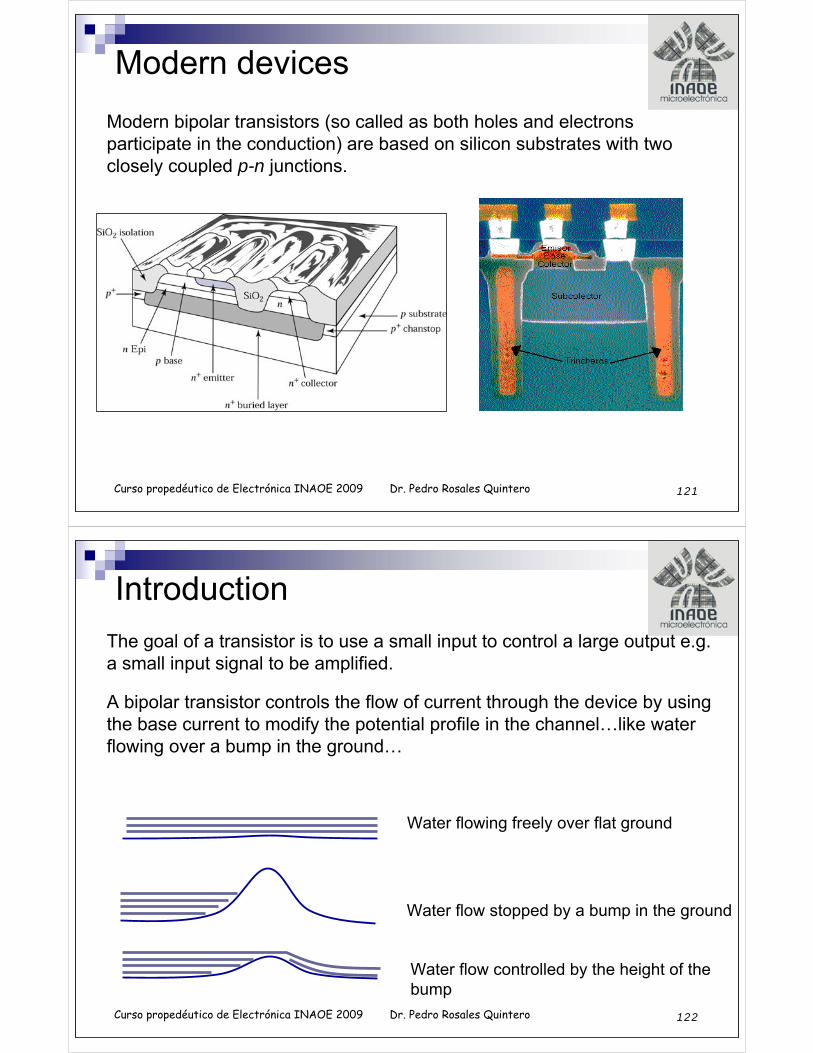
This tiny triangle of plastic, gold and germanium was the first solid-state amplifier
The bipolar transistor was invented in 1947 at Bell labs by Bardeen & Brattain consisting of metal points contacting a germanium substrate. It was later explained by Shockley in 1949 and the three shared the Nobel prize for their work.
Base
Collector
Emitter
121Curso propedéutico de Electrónica INAOE 2009 Dr. Pedro Rosales Quintero
Modern devices
Modern bipolar transistors (so called as both holes and electrons participate in the conduction) are based on silicon substrates with two closely coupled p-n junctions.
122Curso propedéutico de Electrónica INAOE 2009 Dr. Pedro Rosales Quintero
Introduction
The goal of a transistor is to use a small input to control a large output e.g. a small input signal to be amplified.
A bipolar transistor controls the flow of current through the device by using the base current to modify the potential profile in the channel…like water flowing over a bump in the ground…
Water flowing freely over flat ground
Water flow stopped by a bump in the ground
Water flow controlled by the height of the bump
123Curso propedéutico de Electrónica INAOE 2009 Dr. Pedro Rosales Quintero
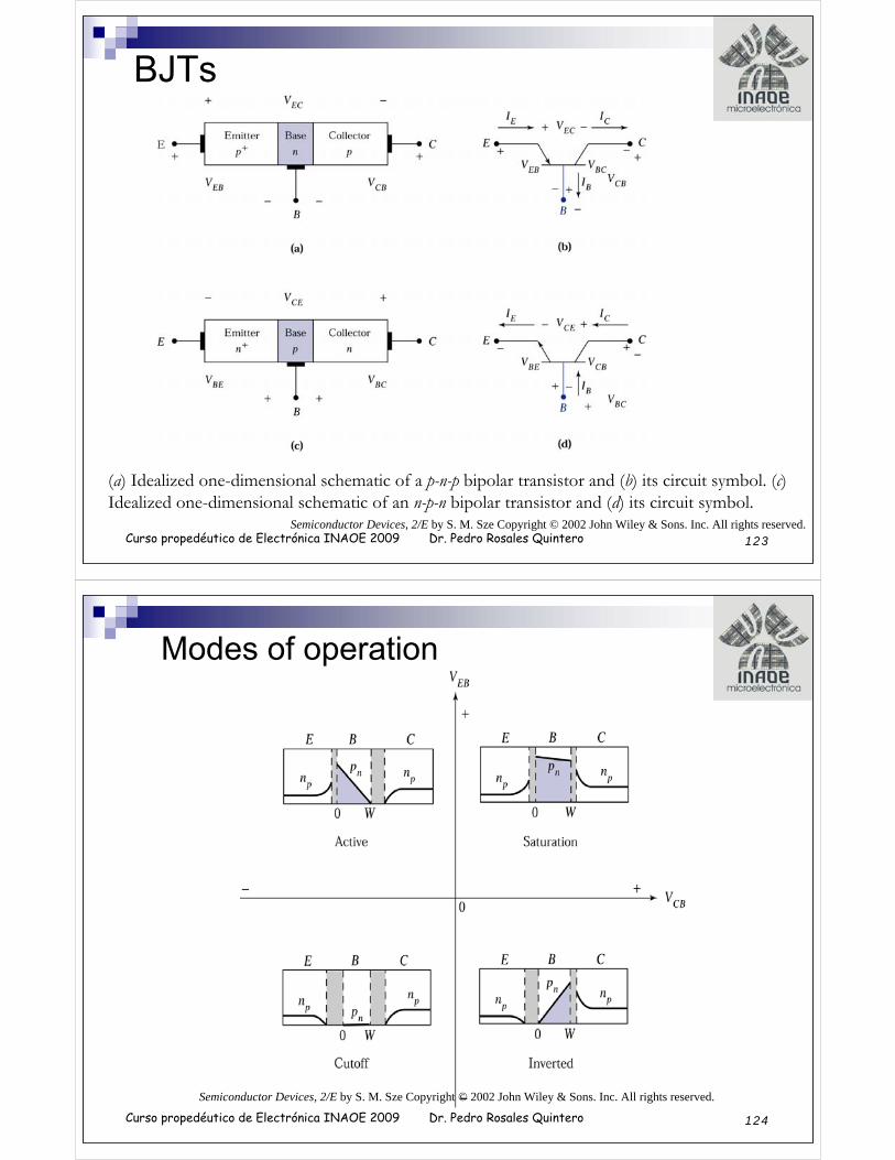
BJTs
Semiconductor Devices, 2/E by S. M. Sze Copyright © 2002 John Wiley & Sons. Inc. All rights reserved.
(a) Idealized one-dimensional schematic of a p-n-p bipolar transistor and (b) its circuit symbol. (c) Idealized one-dimensional schematic of an n-p-n bipolar transistor and (d) its circuit symbol.
124Curso propedéutico de Electrónica INAOE 2009 Dr. Pedro Rosales Quintero
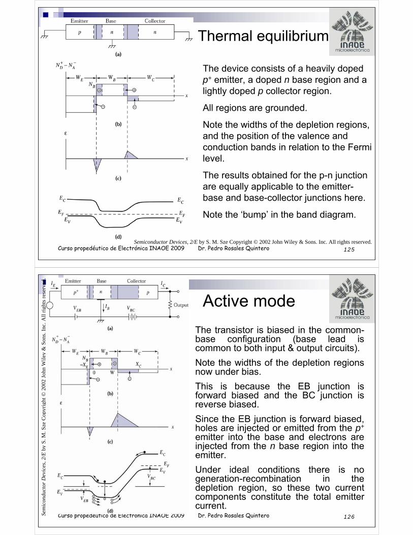
Modes of operation
Semiconductor Devices, 2/E by S. M. Sze Copyright © 2002 John Wiley & Sons. Inc. All rights reserved.
125Curso propedéutico de Electrónica INAOE 2009 Dr. Pedro Rosales Quintero
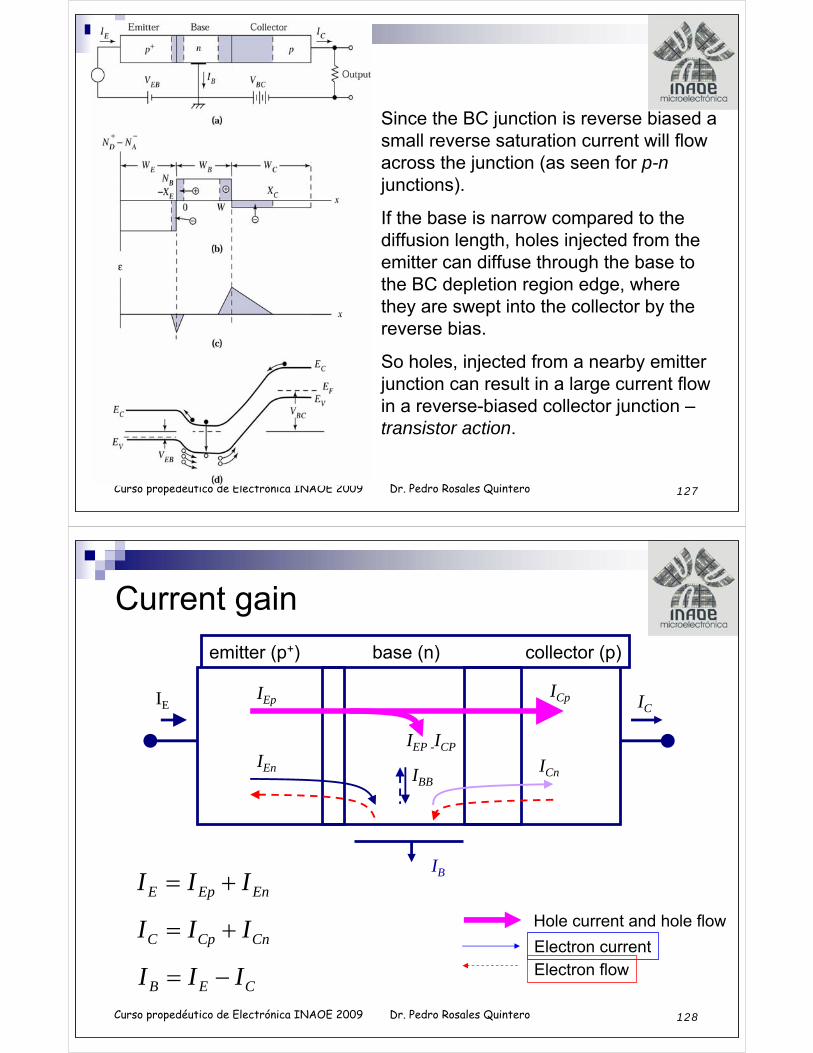
Thermal equilibrium
Semiconductor Devices, 2/E by S. M. Sze Copyright © 2002 John Wiley & Sons. Inc. All rights reserved.
The device consists of a heavily doped p+ emitter, a doped n base region and a lightly doped p collector region.
All regions are grounded.
Note the widths of the depletion regions, and the position of the valence and conduction bands in relation to the Fermi level.
The results obtained for the p-n junction are equally applicable to the emitter-base and base-collector junctions here.
Note the ‘bump’ in the band diagram.
126Curso propedéutico de Electrónica INAOE 2009 Dr. Pedro Rosales Quintero
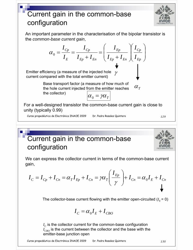
Active mode
Sem
icon
duct
or D
evic
es, 2
/E b
y S
. M. S
zeC
opyr
ight
©20
02 J
ohn
Wil
ey &
Son
s. I
nc. A
ll r
ight
s re
serv
ed.
The transistor is biased in the common-base configuration (base lead is common to both input & output circuits).
Note the widths of the depletion regions now under bias.
This is because the EB junction is forward biased and the BC junction is reverse biased.
Since the EB junction is forward biased, holes are injected or emitted from the p+
emitter into the base and electrons are injected from the n base region into the emitter.
Under ideal conditions there is no generation-recombination in the depletion region, so these two current components constitute the total emitter current.
127Curso propedéutico de Electrónica INAOE 2009 Dr. Pedro Rosales Quintero
Since the BC junction is reverse biased a small reverse saturation current will flow across the junction (as seen for p-njunctions).
If the base is narrow compared to the diffusion length, holes injected from the emitter can diffuse through the base to the BC depletion region edge, where they are swept into the collector by the reverse bias.
So holes, injected from a nearby emitter junction can result in a large current flow in a reverse-biased collector junction –transistor action.
128Curso propedéutico de Electrónica INAOE 2009 Dr. Pedro Rosales Quintero
emitter (p+) base (n) collector (p)
IE IC
IB
Current gain
IEp
IEP -ICP
ICp
ICnIEn IBB
Hole current and hole flow
Electron currentElectron flow
EnEpE III +=
CnCpC III +=
CEB III −=
129Curso propedéutico de Electrónica INAOE 2009 Dr. Pedro Rosales Quintero
Current gain in the common-base configuration
An important parameter in the characterisation of the bipolar transistor is the common-base current gain,
γEmitter efficiency (a measure of the injected hole current compared with the total emitter current)
Base transport factor (a measure of how much of the hole current injected from the emitter reaches the collector)
Tγαα =0
For a well-designed transistor the common-base current gain is close to unity (typically 0.99)
Tα
⎟⎟⎠
⎞⎜⎜⎝
⎛⎟⎟⎠
⎞⎜⎜⎝
⎛
+=
+==
Ep
Cp
EnEp
Ep
EnEp
Cp
E
Cp
I
I
II
I
II
I
I
I0α
130Curso propedéutico de Electrónica INAOE 2009 Dr. Pedro Rosales Quintero
Current gain in the common-base configuration
We can express the collector current in terms of the common-base current gain,
CnECnEp
TCnEpTCnCpC IIII
IIIII +=+⎟⎟⎠
⎞⎜⎜⎝
⎛=+=+= 0αγγαα
The collector-base current flowing with the emitter open-circuited (IE = 0)
CBOEC III += 0α
IC is the collector current for the common-base configurationICBO is the current between the collector and the base with the emitter-base junction open
131Curso propedéutico de Electrónica INAOE 2009 Dr. Pedro Rosales Quintero
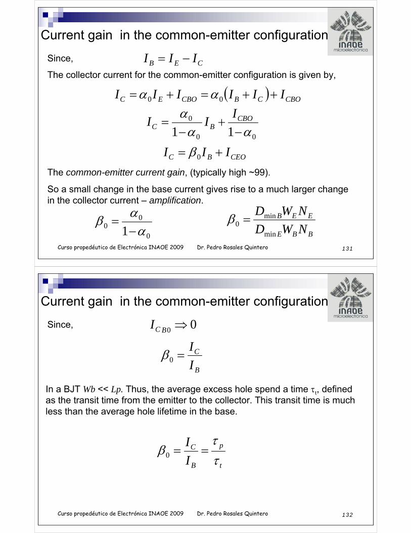
Current gain in the common-emitter configuration
The collector current for the common-emitter configuration is given by,
Since, CEB III −=
( ) CBOCBCBOEC IIIIII ++=+= 00 αα
00
0
11 ααα
−+
−= CBO
BC
III
CEOBC III += 0β
0
00 1 α
αβ−
=
The common-emitter current gain, (typically high ~99).
So a small change in the base current gives rise to a much larger change in the collector current – amplification.
BBE
EEB
NWD
NWD
min
min0 =β
132Curso propedéutico de Electrónica INAOE 2009 Dr. Pedro Rosales Quintero
Current gain in the common-emitter configuration
Since, 00 ⇒BCI
B
C
I
I=0β
t
p
B
C
I
I
ττ
β ==0
In a BJT Wb << Lp. Thus, the average excess hole spend a time τt, defined as the transit time from the emitter to the collector. This transit time is much less than the average hole lifetime in the base.
133Curso propedéutico de Electrónica INAOE 2009 Dr. Pedro Rosales Quintero
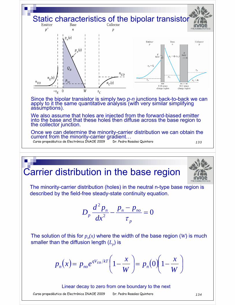
Static characteristics of the bipolar transistor
Since the bipolar transistor is simply two p-n junctions back-to-back we can apply to it the same quantitative analysis (with very similar simplifying assumptions).
We also assume that holes are injected from the forward-biased emitter into the base and that these holes then diffuse across the base region to the collector junction.
Once we can determine the minority-carrier distribution we can obtain the current from the minority-carrier gradient…
134Curso propedéutico de Electrónica INAOE 2009 Dr. Pedro Rosales Quintero
Carrier distribution in the base region
The minority-carrier distribution (holes) in the neutral n-type base region is described by the field-free steady-state continuity equation.
02
2
=−
−p
nonnp
pp
dx
pdD
τ
The solution of this for pn(x) where the width of the base region (W) is much smaller than the diffusion length (Lp) is
( ) ( ) ⎟⎠⎞
⎜⎝⎛ −=⎟
⎠⎞
⎜⎝⎛ −=
W
xp
W
xepxp n
kTqVnon
EB 101
Linear decay to zero from one boundary to the next
135Curso propedéutico de Electrónica INAOE 2009 Dr. Pedro Rosales Quintero
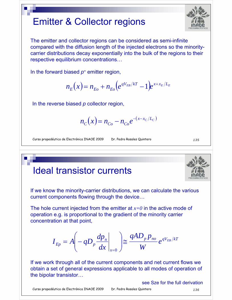
Emitter & Collector regions
The emitter and collector regions can be considered as semi-infinite compared with the diffusion length of the injected electrons so the minority-carrier distributions decay exponentially into the bulk of the regions to their respective equilibrium concentrations…
( ) ( ) EEEB LxxkTqVEoEoE eennxn +−+= 1
In the forward biased p+ emitter region,
( ) ( )CC LxxCoCoC ennxn −−−=
In the reverse biased p collector region,
136Curso propedéutico de Electrónica INAOE 2009 Dr. Pedro Rosales Quintero
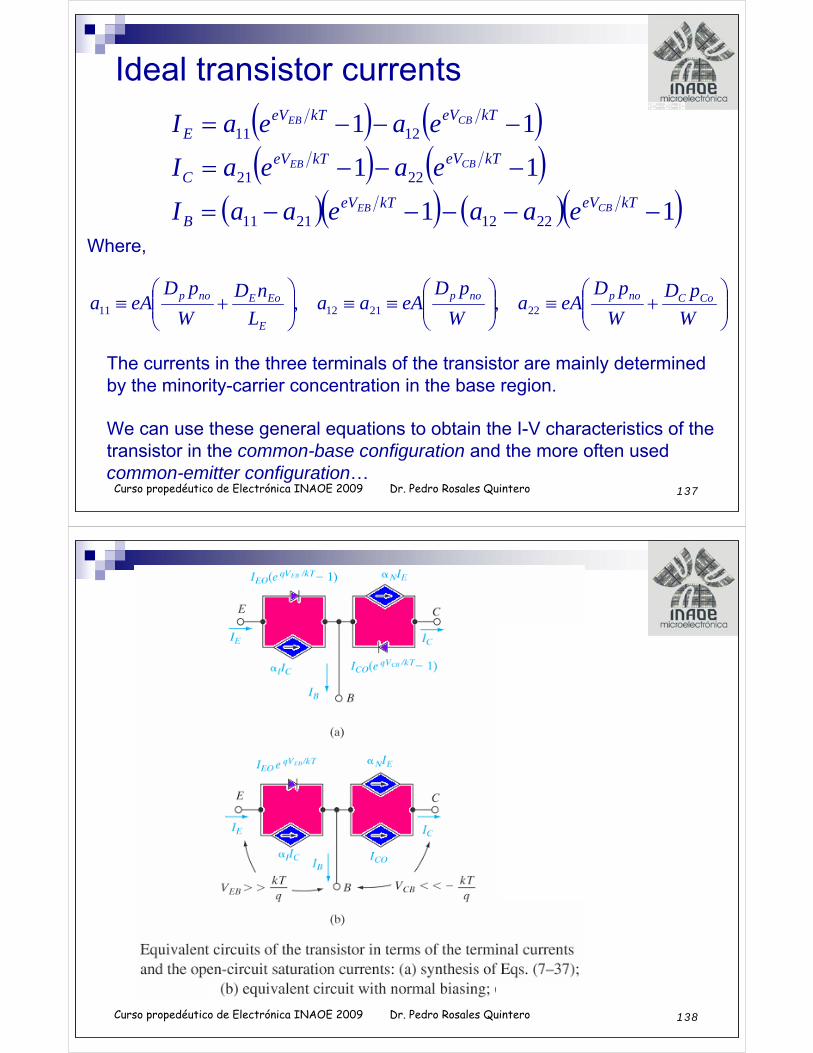
Ideal transistor currents
If we know the minority-carrier distributions, we can calculate the various current components flowing through the device…
kTqVnop
x
npEp
EBeW
pqAD
dx
dpqDAI ≅⎟⎟
⎠
⎞⎜⎜⎝
⎛−=
=0
The hole current injected from the emitter at x=0 in the active mode of operation e.g. is proportional to the gradient of the minority carrier concentration at that point,
If we work through all of the current components and net current flows we obtain a set of general expressions applicable to all modes of operation of the bipolar transistor…
see Sze for the full derivation
137Curso propedéutico de Electrónica INAOE 2009 Dr. Pedro Rosales Quintero
Ideal transistor currents
( ) ( )( ) ( )
( )( ) ( )( )11
11
11
22122111
2221
1211
−−−−−=
−−−=
−−−=
kTeVkTeVB
kTeVkTeVC
kTeVkTeVE
CBEB
CBEB
CBEB
eaaeaaI
eaeaI
eaeaI
Where,
⎟⎟⎠
⎞⎜⎜⎝
⎛+≡⎟⎟
⎠
⎞⎜⎜⎝
⎛≡≡⎟⎟
⎠
⎞⎜⎜⎝
⎛+≡
W
pD
W
pDeAa
W
pDeAaa
L
nD
W
pDeAa CoCnopnop
E
EoEnop22211211 ,,
The currents in the three terminals of the transistor are mainly determined by the minority-carrier concentration in the base region.
We can use these general equations to obtain the I-V characteristics of the transistor in the common-base configuration and the more often used common-emitter configuration…
138Curso propedéutico de Electrónica INAOE 2009 Dr. Pedro Rosales Quintero